
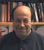
KeyNote Speaker

Lorenzo Faraone (Also: Tutorial Speaker)
The University of Western Australia (Australia)
Director Semiconductor Optoelectronics and Microsystems, Western Australian Centre for (WACSOM)
Topic: Optical MEMS Technologies for Infrared Spectroscopy, Sensing, and Imaging
Abstract: Current research efforts to further improve state-of-the-art infrared (IR) detector and imaging focal plane array (FPA) technologies are focused on reducing system cooling requirements, developing larger-format 2-dimensional imaging FPAs, extending the technology to longer wavelengths, and/or adding so-called multi-colour/hyper-spectral capability, which allows real-time spectral information to be gathered from multiple wavelength bands. Multi/hyper-spectral imaging in defence & aerospace scenarios provides enhanced target detection, improved target recognition, and reduced false alarm rates. In civilian, industrial and commercial arenas, such a technology is applicable to numerous remote sensing spectroscopy/imaging applications in agriculture, medical diagnostics, process control, food security, etc.
This presentation will focus on recent advances in optical MEMS technologies that are capable of providing reduced size, weight and power (SWaP) solutions for field-portable and airborne drone/UAV applications. In particular, a number of micro-electromechanical systems (MEMS) based electrically tuneable Fabry-Perot filter technologies will be presented that are compatible with either individual detectors or large format 2-dimensional imaging IRFPAs. Such a technology can be hybridised with any existing optoelectronic detector/sensing/imaging technology, and is capable of low-voltage tuning across the NIR/SWIR, MWIR or LWIR wavelength bands for field-portable or airborne spectroscopy and/or imaging applications.
Bio: Professor Faraone is a Member of the Order of Australia (AM), and a Fellow of the Institute of Electrical and Electronic Engineers (FIEEE), Australian Academy of Science (FAA) and the Australian Academy of Technological Sciences and Engineering (FTSE). He has published more than 250 international journal papers on his research work, and supervised more than 35 PhD student completions. He is currently Head of the Microelectronics Research Group (MRG) at The University of Western Australia (UWA), and Director of the WA Centre for Semiconductor Optoelectronics and Microsystems (WACSOM). Prior to joining UWA in 1987, he worked primarily in the area of silicon CMOS-based microelectronics and non-volatile memory technology with RCA Labs in Princeton, NJ, USA. Since joining UWA he has worked on compound semiconductor materials and devices, including AlGaN/GaN HEMTs, HgCdTe-based infrared sensor technology and MBE growth, as well as optical MEMS technologies for infrared spectroscopy and imaging applications. His research activities also include mobility spectrum techniques for magneto-transport studies, which allow the transport properties and mobility distributions of individual carriers in multi-layer/multi-carrier semiconductor systems to be determined.
Invited Speakers
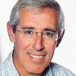
 Tayeb Mohammed-Brahim (Also: Tutorial Speaker)

Université de Rennes (France)
Topic: Silicon: a flexible material for bendable electronics and sensors
Abstract: Directly crystallized deposited silicon at low temperature is shown to be the right material when bendable system including treatment electronics and sensing functions is needed. This is true particularly when process reproducibility, electrical and mechanical reliability of the devices are the most important parameters implying the success of the technology. Indeed, these parameters are the main issues when we need to go beyond the publication of a paper, towards actual commercial application.
Electrical and mechanical performances of microcrystalline silicon thin film transistors and deformation sensors on 25 µm thick flexible plastics under high bending, still 0.75 mm curvature radius, are presented. These devices are fabricated directly on this substrate at a maximum temperature of 180°C.
Bio: Tayeb Mohammed-Brahim is currently professor in Rennes 1 University (France), Head of Microelectronics & Microsensors Department of the Institute of Electronics and Telecommunications of Rennes and Director of the Common Center on Microelectronics in the west of France. He got his PhD (Doctorat d’Etat) in Paris-XI University (France) and he founded the thinfilm Laboratory in Algiers University (Algeria). Then he moved to Caen University (France) where he created the reliability Laboratory. After that and since 2000, he moved to Rennes University where he became the head of Microelectronics Group becoming the Microelectronics and Microsensors Department after 2002.
He is mainly involved in low temperature fabrication of thin film electronic devices for flexible electronics and in the fabrication of sensors. Previously he activated a lot on chemical and biologic sensors for the measurement of pH, the detection of DNA and the quantification of proteins. Presently, his main activities focus on mechanical sensors for health applications. He is author of more than 300 papers on these different fields.
 Patrick Fay (Also: Tutorial Speaker)

University of Notre Dame (USA)
Topic: Beyond Power: III-N Devices for Low-Power Systems, Millimeter-Wave Applications, and More
Abstract: Devices based on GaN and related III-N materials are increasingly well established in RF power applications, and are under active research and development for power conversion and control applications. However, the unique material properties of the III-Ns make them a promising basis for applications well beyond these traditional applications. Novel device concepts that harness these material properties in conjunction with unconventional operational physics are being explored to serve needs in applications as diverse as millimeterwave and THz electronics and sensing, low-power systems, and ultra-scaled low-power logic. Devices exploiting interband tunneling in III-N heterostructures for low-power logic, as well as impact ionization and plasma-wave propagation in GaN 2DEGs for millimeter-wave and THz sensing and electronics are under active investigation to provide new levels of performance.
Bio: Patrick Fay is a Professor in the Dept. of Electrical Engineering at the University of Notre Dame. He received a Ph.D. in electrical engineering from the University of Illinois at Urbana-Champaign in 1996. His research interests include the design, fabrication, and characterization of compound semiconductor electronic devices and circuits, as well as high-speed optoelectronic devices and optoelectronic integrated circuits for fiber optic telecommunications. His research also includes the development and use of micromachining techniques for the fabrication of microwave through sub-millimeter-wave components and packaging. He established the High Speed Circuits and Devices Laboratory at Notre Dame that houses comprehensive device and circuit test capabilities. He also oversaw the design, construction, and commissioning of the class 100 cleanroom housed in Stinson-Remick Hall at Notre Dame, and has served as the director of this facility since 2003. Prof. Fay is a fellow of the IEEE, has published 9 book chapters, more than 130 articles in refereed scientific journals, and more than 180 conference proceedings.
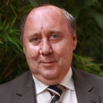
 Fernando Guarín (Also: Tutorial Speaker)

Global Foundries (USA)
Topic: Leveraging semiconductor technology for the benefit of society
Abstract: Electron devices, thanks to relentless scaling, coupled along with advances in material science, have enabled the exponential growth of the information technologies that have transformed society. This increased information content gives us a unique path to alleviate and find solutions to the problems of many of the most important issues facing the world today. These advances must remind us that we are all now connected – economically, technically and socially. But we are also learning that just being connected may not be sufficient. We must solve many problems. As engineers, we have the knowledge and the responsibility to do so. The level of instrumentation grows daily with ever increasing intelligence and ability to communicate and automate many processes and industries in what is now known as the Internet of Things (IoT). Thanks to these advances the world is smaller and flatter. The reality of living in a globally integrated world is upon us and is presenting us with many opportunities and challenges. In this talk, we will discuss how Semiconductor technology and electron devices have benefited society and the world in which we live. The multiple advances in devices and materials have provided us with unprecedented amounts of information at continually decreasing costs. We will provide tangible evidence that illustrates how electron devices are influencing society, changing our interaction with other people near and far, while providing many people the ability to have access to light and information technology even in the most remote corners of the planet. We must leverage these advances to expand educational opportunities while helping to preserve a sustainable and greener environment. We will provide information on initiatives and access to funding for engineering projects at the local level. Ultimately we must always bear in mind that the large number of scientific and technological advances must produce tangible results for the benefit and progress of humanity.
Bio: Dr. Fernando Guarín is a Distinguished Member of Technical Staff at Global Foundries in East Fishkill NY and Adjunct Lecturer at SUNY New Paltz. He retired from IBM’s SRDC after 27 years as Senior Member of Technical Staff. He earned his BSEE from the “Pontificia Universidad Javeriana”, in Bogotá, Colombia, the M.S.E.E. degree from the University of Arizona, and the Ph.D. in Electrical Engineering from Columbia University, NY He has been actively working in microelectronic reliability for over 35 years.
From 1980 until 1988 he worked in the Military and Aerospace Operations division of National Semiconductor Corporation. In 1988 he joined IBM’s microelectronics division where he worked in the reliability physics and modeling of Advanced Bipolar, CMOS and Silicon Germanium BiCMOS technologies.
Dr. Guarín is an IEEE Fellow, Distinguished Lecturer for the IEEE Electron Device Society, where he has served in many capacities including; member of the IEEE’s EDS Board of governors, chair of the EDS Education Committee, Secretary for EDS. He is the EDS President-Elect 2016-2017.
 Mircea Guina
Tampere University of Technology (Finland)
Topic: III-V/Si integration: technological advances and new application perspectives
Abstract: A review of two major directions for integrating optoelectronics and microelectronics technology platforms is presented. As a first approach, we will discuss progress concerning the hybrid integration of silicon photonics, in particular silicon-on-insulator technology, with III-V optoelectronic components. Secondly, we review recent progress concerning direct integrating of III-V alloys on Si by so called heteroepitaxy technology. Applications outlined include realization of integrated optical transceiver for data communication at several hundreds of GB/s and development of multi-wavelength Si-integrated light sources for spectroscopy.
Bio: Mircea Guina received the Ph.D. degree in physics from the Tampere University of Technology, Tampere, Finland, in 2002. In 2008, he was appointed as the Professor and Head of the III–V Optoelectronics Group at the Optoelectronics Research Centre, Tampere University of Technology. He conducts scientific work related to molecular beam epitaxy of novel optoelectronic heterostructures and devices, and their applications. His current projects are concerned with the development of uncooled lasers, amplifiers, and modulators for hybrid-PICs, ordered nanostructures for quantum optics, epitaxy of III-Bi-V alloys, the development of high-power semiconductor lasers (VECSELs and MOPAs), and the development of ultrahigh efficiency multijunction solar cells based on GaInNAsSb-alloys. He has published more than 120 journal papers, several book chapters, holds four international patents, has several position of trust in COST Actions and scientific boards, and has given numerous invited talks at major optoelectronics conferences. He is the Director of the International Summer School “New Frontiers in Optical Technologies,” which he established in 2001.
 Libor Rufer
University of Grenoble / TIMA Laboratory (France)
Topic: Approaches to the Design, Fabrication, and Test of Electroacoustic Micro-transducers
Abstract: Silicon-based microphones are nowadays well-established MEMS components produced by strong industrial actors. The fabrication of such acoustic sensors is based on a dedicated technology fulfilling all designed parameters. On the other hand, the development of such a technology processes is costly and time-consuming. In this paper, we will present approaches based on technologies readily available to small companies and academic institutions. We will show, on several examples, a design process of acoustic micro-transducers fabricated through generic technologies. Focused will be a CMOS-MEMS process applied to the realization of suspended diaphragms that can be part of transducers with piezoresistive, electrostatic, or electrodynamic transduction. We will also briefly present a testing technique that can be used for acoustic sensors calibration. This technique has a special interest for sensors with a frequency response exceeding the typical audible range.
Bio: Libor Rufer received his Engineer degree from the Faculty of Electrical Engineering, Prague and his Ph.D. in Acoustics from Czech Technical University, Prague, Czech Republic. He obtained his DEA diploma (Diplôme d’Etudes Approfondies, eq. Master) in Acoustics from Ecole Centrale, Lyon, France and the HDR (Habilitation à Diriger des Recherches) diploma in physics from Joseph Fourier University, Grenoble, France. Until 1993, he was with the Faculty of Electrical Engineering at the Czech Technical University, Prague. Since then, he is a researcher with the Joseph Fourier University, Grenoble, France. In 1998, he joined the TIMA Laboratory. Currently, he is member of its MNS (Micro- Nano- Systems) Group. His expertise is mainly in MEMS-based sensors and actuators, electro-acoustic and electro-mechanical transducers modeling, design, and applications of these devices in different fields as consumer, biomedical or RF.
 Yeshaiahu Fainman (Also: Tutorial Speaker)
University of California San Diego (USA)
Topic: Nanoscale Light-Emitters
Abstract: Nanocavity light-emitters with high spontaneous emission factors, β, have attracted considerable attention in the past decade in light of their technical applications ranging from optical interconnects, sensing and imaging to fundamental research on thresholdless lasers quantum cavity electrodynamics. Theoretically a high- β nanolaser is more energy efficient as most spontaneous emission is funneled into the lasing mode, resulting in an extremely low lasing threshold. In this talk we will focus on three promising candidates for the next generation of densely packed chip-scale photonic circuits: metal-clad subwavelength lasers, coaxial lasers and luminescent hyperbolic metamaterials. We will summarize the recent research efforts in the theory, design, fabrication, and characterization of such devices.
Bio: Professor Fainman eceived the Ph. D. from Technion in 1983. He is a Cymer Professor of Advanced Optical Technologies and Distinguished Professor of ECE at the University of California, San Diego (UCSD). His current research involves near field optical science and technology, nanophotonics, nanolasers, nanoiplasmonics and ultrafast optics. He is a Fellow of OSA, IEEE, and SPIE. He Chaired, co-Chaired and served on numerous program committees for various conferences for OSA, IEEE/LEOS, and SPIE. He is a recipient of the Miriam and Aharon Gutvirt Prize, Technion, Haifa, Israel (1982), Lady Davis Fellowship (2006), Brown award (2006), Gabor Award (2012) and E. Leith Medal (2015). He was a General Chair for Inaugural OSA Topical Meeting on Nanophotonics for Information Systems in 2005 and served as a topical editor and board member for various journals. He contributed over 250 manuscripts in peer review journals and over 450 conference presentations and conference proceedings.
 Cor L. Claeys (Also: Tutorial Speaker)
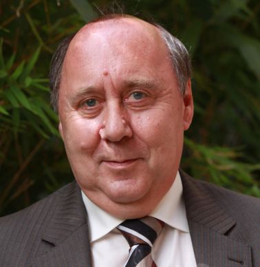
IMEC (Belgium)
Topic: Random Telegraph Signal Noise in Advanced High Performance and Memory Devices
Abstract: Random Telegraph Signal noise has been extensively studied for more than 30 years and gained high interest in recent years due to its importance for scaled down technologies. This review will demonstrate the power of RTS for single defect characterization. Present understanding of the device physics and evolutions in RTS characterization are highlighted. Special attention is given to RTS in memory devices such as DRAMS, ReRAM, planar (2D) and vertical (3D) flash.
Bio: Cor Claeys received the Ph.D. degree from KU Leuven in Belgium, where he is Professor since 1990. At imec he is presently Director of Advanced Semiconductor Technologies responsible for strategic relations. His main interests are silicon technology, device physics, low frequency noise phenomena, radiation effects and defect engineering and material characterization. He co-edited a book on “Low Temperature Electronics” and “Germanium-Based Technologies: From Materials to Devices” and wrote monographs on “Radiation Effects in Advanced Semiconductor Materials and Devices” and “Fundamental and Technological Aspects of Extended Defects in Germanium”. Two of these books have translated in Chinese. He authored and coauthored 14 book chapters, over 1000 conference presentations and more than 1200 technical papers. He is also editor or co-editor of 60 Conference Proceedings. Prof. Claeys is a Fellow of the Electrochemical Society and of IEEE. He was the Founder of the IEEE Electron Devices Benelux Chapter, Chair of the IEEE Benelux Section, an elected AdCom Member of the Electron Devices Society and the EDS Vice President for Chapters and Regions. He was EDS President in 2008-2009. He was as Division Director on the IEEE Board of Directors in 2012-2013. He is a recipient of the IEEE Third Millennium Medal and in 2013 he received the IEEE EDS Distinguished Service Award. Within the Electrochemical Society, he was the Chair of the Electronics & Photonics Division from 2001 to 2003. In 2004, he received the Electronics & Photonics Division Award.
Tutorial Speakers
 Enrico Sangiorgi

Università di Bologna (Italy)
Topic: Micro- and nano-power management circuit systems for energy harvesting
Abstract: The present interest on pervasive sensor networks and the steady development of electronic devices with low power consumption motivates the research on electronic systems capable of harvesting energy from the surrounding environment. In this scenario, mechanical vibrations, thermal gradients, and photovoltaics represent the most promising power sources.
A special care has to be devoted to the design of power conversion and management circuits for energy harvesting applications where, in many practical cases, the available power is often as low as few µW. This talk will review a series of design techniques that ensure ultra-low intrinsic consumptions and pursue effective trade-offs with conversion efficiency. Practical cases based on both integrated and off-the-shelf electronics will be discussed.
Bio: Enrico Sangiorgi received the Laurea degree from the University of Bologna in 1979. He has been a Visiting Scientist at Stanford University and Bell Laboratories, Murray Hill, NJ. In 1993, he was appointed Full Professor of Electronics at the University of Udine, Italy. In 2002, he joined the University of Bologna, where he has been Dean of the Faculty of Engineering, Director of the EE Department “Guglielmo Marconi” and currently Vice-Rector for Teaching and Education. He has been Editor of Electron Device Letters, on the editorial board for the Transactions on Electron Devices and Journal of Photo-Voltaics. His research covers various device modeling and characterization aspects. Enrico Sangiorgi is a Distinguished Lecturer and a Fellow of the IEEE; he has been Chairman of the EDS TCAD Technical Committee, member of the Cledo Brunetti Award , the Education Award, and the Fellow Committees of the EDS.
Lorenzo Faraone (Also: Keynote Speaker)
The University of Western Australia (Australia)
Director Semiconductor Optoelectronics and Microsystems, Western Australian Centre for (WACSOM)
Topic: Infrared optoelectronics technology: Materials and devices for detectors and imaging applications
Abstract: This tutorial will review the current status and future trends in infrared optoelectronics technology: from material requirements to detector and imaging focal plane array technologies, as well as applications in areas such as defence, security & aerospace, food & agriculture, biomedical diagnostics, process control, etc. In particular, this tutorial will focus on high-performance technologies suitable for remote sensing and spectroscopic applications, as well as large-format 2-D focal plane array technologies for night vision and hyperspectral imaging applications.
The tutorial will be presented in a format that should be suitable for anyone interested in the general area of infrared optoelectronics technology, and will be at a level suitable for non-specialists. The only requirement will be a general knowledge of semiconductor materials and devices at a university undergraduate level.
Bio: Professor Faraone is a Member of the Order of Australia (AM), and a Fellow of the Institute of Electrical and Electronic Engineers (FIEEE), Australian Academy of Science (FAA) and the Australian Academy of Technological Sciences and Engineering (FTSE). He has published more than 250 international journal papers on his research work, and supervised more than 35 PhD student completions. He is currently Head of the Microelectronics Research Group (MRG) at The University of Western Australia (UWA), and Director of the WA Centre for Semiconductor Optoelectronics and Microsystems (WACSOM). Prior to joining UWA in 1987, he worked primarily in the area of silicon CMOS-based microelectronics and non-volatile memory technology with RCA Labs in Princeton, NJ, USA. Since joining UWA he has worked on compound semiconductor materials and devices, including AlGaN/GaN HEMTs, HgCdTe-based infrared sensor technology and MBE growth, as well as optical MEMS technologies for infrared spectroscopy and imaging applications. His research activities also include mobility spectrum techniques for magneto-transport studies, which allow the transport properties and mobility distributions of individual carriers in multi-layer/multi-carrier semiconductor systems to be determined.
 Mehmet Kaynak (Also: INSCIT Invited Speaker)
Innovations for High Performance Microelectronics – IHP (Germany)
Topic: Future of SiGe BiCMOS Technologies with “More-than-Moore” Modules for mm-wave and THz Applications
Abstract: In last decade, SiGe BiCMOS technologies open a new cost-efficient market at mm-wave frequencies. Starting with the commercial use of automotive radars at 77 GHz, the market now has a strong interest on radar, sensor and imaging products at mm-wave and sub-THz frequencies. The latest developments on SiGe HBTs with fmax of beyond 600 GHz boosts the research and development effort on circuit and system area to take share from the new market. In parallel to the developments on SiGe HBT performance, “More-than-Moore” path, which covers all the additional functionalities to the standard CMOS process (i.e. MEMS devices, microfluidics, etc…), allows to realize multi-functional circuits and systems. In this talk, the latest developments regarding the high-speed devices and circuits based on SiGe HBTs will be discussed. The “More-than-Moore” modules for multi-functional device and circuits will also be one of the core topic of discussion.
Bio: Dr. –Ing Mehmet Kaynak received his B.S degree from Electronics and Communication Engineering Department of Istanbul Technical University (ITU) in 2004, took the M.S degree from Microelectronic program of Sabanci University, Istanbul, Turkey in 2006 and received the PhD degree from Technical University of Berlin, Berlin Germany in 2014. He joined the technology group of IHP Microelectronics, Frankfurt (Oder), Germany in 2008. Dr. Kaynak has received the young scientist award of Leibniz institute for the year of 2014. Since 2015, he is acting as the department head of technology group at IHP, Germany and network faculty member at Sabanci University, Turkey.
Tayeb Mohammed-Brahim (Also: Invited Speaker)
Université de Rennes (France)
Topic: Flexible electronics: the new way towards friendly applications
Abstract: Flexible electronics is the new paradigm, enlarging the applications of electronics to new fields as health, transport, robotics,…Huge works are devoted now to this electronics involving great number of ways. Different materials from known silicon to multiple organic materials and renewed metal oxides are used. Different techniques from known photolithography to new deposition in solution ones are used also. The main drawback of a lot of ways is the lack of reproducibility in the process and/or of reliability of the devices.
The tutorial is a critical review of these ways focusing on the process reproducibility and the device reliability. Examples of the most important success in this story are given. Applications of the devices in different fields, health particularly, are briefly described.Tayeb Mohammed-Brahim is currently professor in Rennes 1 University (France), Head of Microelectronics & Microsensors Department of the Institute of Electronics and Telecommunications of Rennes and Director of the Common Center on Microelectronics in the west of France. He got his PhD (Doctorat d’Etat) in Paris-XI University (France) and he founded the thinfilm Laboratory in Algiers University (Algeria). Then he moved to Caen University (France) where he created the reliability Laboratory. After that and since 2000, he moved to Rennes University where he became the head of Microelectronics Group becoming the Microelectronics and Microsensors Department after 2002.
Bio: He is mainly involved in low temperature fabrication of thin film electronic devices for flexible electronics and in the fabrication of sensors. Previously he activated a lot on chemical and biologic sensors for the measurement of pH, the detection of DNA and the quantification of proteins. Presently, his main activities focus on mechanical sensors for health applications. He is author of more than 300 papers on these different fields.
Cor L. Claeys (Also: Invited Speaker)
IMEC (Belgium)
Topic: Challenge of Advanced Semiconductor Devices for future CMOS Technologies
Abstract: Advanced devices are not only driven by minimum device geometry, performance enhancement and cost issues, but also require a low power consumption. This is achieved by optimizing process modules, introduction of new materials and modified device concepts. This led to the implementation of stress engineering, ultra-shallow junctions, gate-stacks with EOT’s below 1 nm, optimization of process sequences (e.g. gate-first versus replacement gate or gate-last), raised source/drain for resistance control, etc. Improved drive currents and electrostatic control triggered the exploration of Multi-gate devices (MuGFETs). For scaled-down technologies, FD technologies with ultrathin body and buried oxide (UTBB SOI) have demonstrated their strong potential down to the 14 nm mode. At those dimension there exists a strong competition between planar UTBB SOI and bulk FinFETs. Tunnel-FETs (TFETs), relying on band-to-band-tunneling and allowing to achieve steep subthreshold swings are studied. Both horizontal and vertical TFET approaches are emerging as post-CMOS alternatives. Further scaling leads to gate-all-around and nanowire devices. Optimized epitaxial growth techniques resulted in the fabrication of Ge (p-channel), III-V (n-channel) or hybrid Ge/III-V devices on a Si substrate. These high mobility materials are also implemented in TFET and nanowire structures. Beyond CMOS technologies will be based on alternative technologies such as 2D materials, quantum computing and spintronics. The paper reviews the status and the challenges of several of these advanced technologies and outlines potential limitations.
Bio: Cor Claeys received the Ph.D. degree from KU Leuven in Belgium, where he is Professor since 1990. At imec he is presently Director of Advanced Semiconductor Technologies responsible for strategic relations. His main interests are silicon technology, device physics, low frequency noise phenomena, radiation effects and defect engineering and material characterization. He co-edited a book on “Low Temperature Electronics” and “Germanium-Based Technologies: From Materials to Devices” and wrote monographs on “Radiation Effects in Advanced Semiconductor Materials and Devices” and “Fundamental and Technological Aspects of Extended Defects in Germanium”. Two of these books have translated in Chinese. He authored and coauthored 14 book chapters, over 1000 conference presentations and more than 1200 technical papers. He is also editor or co-editor of 60 Conference Proceedings. Prof. Claeys is a Fellow of the Electrochemical Society and of IEEE. He was the Founder of the IEEE Electron Devices Benelux Chapter, Chair of the IEEE Benelux Section, an elected AdCom Member of the Electron Devices Society and the EDS Vice President for Chapters and Regions. He was EDS President in 2008-2009. He was as Division Director on the IEEE Board of Directors in 2012-2013. He is a recipient of the IEEE Third Millennium Medal and in 2013 he received the IEEE EDS Distinguished Service Award. Within the Electrochemical Society, he was the Chair of the Electronics & Photonics Division from 2001 to 2003. In 2004, he received the Electronics & Photonics Division Award.
Fernando Guarín (Also: Invited Speaker)
Global Foundries (USA)
Topic: Reliability challenges for the qualification of Leading Edge CMOS Technologies
Abstract: This presentation will address some of the key reliability challenges during the qualification of a 14nm SOI CMOS technology. Some of the issues are driven by self heating in SOI and some by the latest trends in semiconductor fabrication as we continue to scale and deal with the new reliability challenges introduced by the use of High K Metal Gate (HKMG) and FinFet devices. We will discuss the reliability impact and the qualification activities driven by the introduction of SOI and new materials. . The path to maintaining the advanced CMOS scaling cadence and new reliability limiting factors will be examined from the reliability perspective. A closer look will be given to Hot Carriers, Bias Temperature Instabilities and Gate Dielectric Integrity. The characterization, models and qualification methodologies will be put in the required perspective for the successful qualification and transfer of leading edge technologies to a manufacturing environment.
Bio: Dr. Fernando Guarín is a Distinguished Member of Technical Staff at Global Foundries in East Fishkill NY and Adjunct Lecturer at SUNY New Paltz. He retired from IBM’s SRDC after 27 years as Senior Member of Technical Staff. He earned his BSEE from the “Pontificia Universidad Javeriana”, in Bogotá, Colombia, the M.S.E.E. degree from the University of Arizona, and the Ph.D. in Electrical Engineering from Columbia University, NY He has been actively working in microelectronic reliability for over 35 years.
From 1980 until 1988 he worked in the Military and Aerospace Operations division of National Semiconductor Corporation. In 1988 he joined IBM’s microelectronics division where he worked in the reliability physics and modeling of Advanced Bipolar, CMOS and Silicon Germanium BiCMOS technologies.
Dr. Guarín is an IEEE Fellow, Distinguished Lecturer for the IEEE Electron Device Society, where he has served in many capacities including; member of the IEEE’s EDS Board of governors, chair of the EDS Education Committee, Secretary for EDS. He is the EDS President-Elect 2016-2017.
Shaya Fainman (Also: Invited Speaker)
University of California San Diego (USA)
Topic: Nanophotonics Technology and Applications
Abstract: Various future system applications that involve photonic technology rely on our ability to integrate it on a chip to augment and/or interact with other signals (e.g., electrical, chemical, biomedical, etc.). For example, future computing and communication systems will need integration of photonic circuits with electronics and thus require miniaturization of photonic materials, devices and subsystems. Another example, involves integration of microfluidics with nanophotonics, where former is used for particle manipulation, preparation and delivery, and the latter in a large size array form parallel detection of numerous biomedical reactions useful for healthcare applications. To advance the nanophotonics technology we established design, fabrication and testing tools. The design tools need to incorporate not only the electromagnetic equations, but also the material and quantum physics equations to include near field interactions. These designs are integrated with device fabrication and characterization to validate the device concepts and optimize their performance. Our research work emphasizes the construction of passive (e.g., engineered composite metamaterials, filters, etc.) and active (e.g., nanolasers) components on-chip, with the same lithographic tools as electronics. In this talk, we discuss some of the passive metamaterials and devices that recently have been demonstrated in our lab. These include our recent results on nanoscale engineering optical nonlinearities with SOI material platform and design, fabrication and testing of nanolasers constructed using metal-dielectric-semiconductor resonators confined in all three dimensions.
Bio: Professor Fainman eceived the Ph. D. from Technion in 1983. He is a Cymer Professor of Advanced Optical Technologies and Distinguished Professor of ECE at the University of California, San Diego (UCSD). His current research involves near field optical science and technology, nanophotonics, nanolasers, nanoiplasmonics and ultrafast optics. He is a Fellow of OSA, IEEE, and SPIE. He Chaired, co-Chaired and served on numerous program committees for various conferences for OSA, IEEE/LEOS, and SPIE. He is a recipient of the Miriam and Aharon Gutvirt Prize, Technion, Haifa, Israel (1982), Lady Davis Fellowship (2006), Brown award (2006), Gabor Award (2012) and E. Leith Medal (2015). He was a General Chair for Inaugural OSA Topical Meeting on Nanophotonics for Information Systems in 2005 and served as a topical editor and board member for various journals. He contributed over 250 manuscripts in peer review journals and over 450 conference presentations and conference proceedings.