KeyNote Speaker
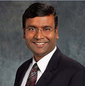
Rajiv Joshi
IBM Thomas J. Watson Research Center (USA)
Topic: From Low Power to Predictive Analytics – Beyond Guessing
Abstract:Moore’s law drives lowering cost/function ratio and thus pushes addition of more functions on a chip. This requires reduction in power. In Internet of Everything (IoE), System on Chip (SOC), flexible electronics, 3D printing the drive towards low power while maintaining functionality will be essential. Also power has become the key driving force in high performance processor designs as the frequency scale-up is reaching saturation. In order to achieve low power system, circuit and technology co-design is essential. This talk focuses on pros and cons analysis of technology and circuit techniques from power perspective and various techniques to exploit lower power. The talk highlights fundamentals and the direction for low power optimization such as reduction in active, leakage, short circuit power and collision power will continue to be the focal area for in the scaled world. Conventional and advanced techniques (e.g. clock gating, power gating, longer channel, multi-Vt design, stacking, header-footer device techniques and new developments etc.) will be described for logic and memories. Finally key challenges in achieving low power will be described. As the technology pushes towards sub-14nm era, process variability and geometric variation in devices can cause variation in power, performance and functionality. Predictive Analytics to capture systematic and random variation and to aid in robust design optimization in nm regime will be discussed. Also the talk will describe future growth directions and role of such predictive algorithms.
Bio: Dr. Rajiv V. Joshi is a research staff member at T. J. Watson research center, IBM. He received his B.Tech I.I.T (Bombay, India), M.S (M.I.T) and Dr. Eng. Sc. (Columbia University). His novel interconnects processes and structures for aluminum, tungsten and copper technologies which are widely used in IBM for various technologies from sub-0.5µm to 14nm. He has led successfully pervasive statistical methodology for yield prediction and also the technology-driven SRAM at IBM Server Group. He commercialized these techniques. He received 3 Outstanding Technical Achievement (OTAs), 3 highest Corporate Patent Portfolio awards for licensing contributions, holds 57 invention plateaus and has over 215 US patents and over 350 including international patents. He has authored and co-authored over 185 papers. He is recipient of 2015 BMM award. He is inducted into New Jersey Inventor Hall of Fame in Aug 2014 along with pioneer Nikola Tesla. He is a recipient of 2013 IEEE CAS Industrial Pioneer award and 2013 Mehboob Khan Award from Semiconductor Research Corporation. He is a member of IBM Academy of technology and master inventor. He is Distinguished Lecturer for IEEE CAS and EDS society. He is IEEE and ISQED fellow and distinguished alumnus of IIT Bombay. He serves as an Associate Editor of TVLSI. He served on committees of ISLPED (Int. Symposium Low Power Electronic Design), IEEE VLSI design, IEEE CICC, IEEE Int. SOI conference, ISQED and Advanced Metallization Program committees. He served as a general chair for IEEE ISLPED. He is an industry liaison for universities as a part of the Semiconductor Research Corporation. Also he is in the industry liaison committee for IEEE CAS society.
Invited Speakers
Rajeev Ranjan (Also: Tutorial Speaker)
Cadence Design System, Inc. (USA)
Topic: Formal Technology in Modern SoC Flow: Establishing Correctness for Functionality and Security
Abstract: Over the last decade, formal verification technology has made significant impact in bringing quality and productivity gains in SoC design and verification flow – ranging from architectural modeling to RTL development to SoC integration all the way to post-silicon debugging. Today, a variety of targeted verification tasks, e.g. register verification, x-propagation verification, connectivity verification, etc. can be performed solely by formal verification technology without depending on a complementary simulation flow. Verifying security attributes of an SoC is emerging as a challenging area as the IoT era dawns upon us. While the security risks in a system pertain to potential flaws in both hardware and software components, establishing hardware security is critical, because it forms the foundation for secure applications and a security hole in hardware implementation can compromise the entire system.
In this talk, we will first provide a brief overview of formal technology and its applications, followed by a broader discussion on the scalable methods of applying formal technology for hardware security verification.
Bio: Rajeev Ranjan is leading the business development efforts of a newly formed business unit at Cadence following the acquisition of Jasper Design Automation, where he was the CTO and was responsible for developing Jasper’s overall technology vision and driving the business value of formal.
Rajeev has been active in the area of formal verification for over 20 years. He has served in the organization and program committee of many international conferences including DAC, ICCAD, FMCAD, and CHARME. He has published numerous articles and has 12 patents in the area of functional verification. Rajeev received his Bachelor’s degree from Indian Institute of Technology, Kanpur (aka IIT Kanpur), his Master’s degree from University of Illinois at Urbana-Champaign (aka UIUC), and his doctorate degree from University of California at Berkeley (aka UC Berkeley). He also has an MBA degree from Wharton School of Business with a focus on entrepreneurial management and finance.
Jeffrey Bokor
UC Berkeley (USA)
Topic: Speed and Reliability of Nanomagnetic Logic (NML) Technology
Abstract: Nanomagnetic logic (NML) is an alternative to electron charge-based information processing for energy efficient computing applications. However, experiments indicate that nanomagnets are susceptible to thermal and lithographic noise, resulting in logical errors during signal transmission and computation. Here, we study the origins of errors in NML and present a technique for reducing error rates based on anisotropy engineering. Using photoelectron emission microscopy (PEEM), we verify the functionality and error-immunity properties of anisotropy-engineered nanomagnets in NML applications. Further, we use time-resolved PEEM to follow the sub-nanosecond dipolar coupling signal propagation dynamics in optimized chains with 100 ps time resolution as they are cycled with nanosecond field pulses at a rate of 3 MHz. A switching time for individual nanomagnetic elements near 100 ps is observed. These experiments, and accompanying macro-spin and micromagnetic simulations, provide deeper insight into the underlying physics of NML architectures operating on nanosecond timescales and help identify relevant engineering parameters to optimize performance and reliability.
Bio: Jeffrey Bokor is the Paul R. Gray Distinguished Professor of Engineering in the department of Electrical Engineering and Computer Sciences at UC Berkeley. In 2012, he was named Associate Dean for Research in the UC Berkeley College of Engineering. From 2004 until 2012, Prof. Bokor held a joint appointment as Deputy Director for Science at the Molecular Foundry, a nanoscale science research center at Lawrence Berkeley National Laboratories (LBNL). He currently holds a joint appointment as Senior Scientist in the Materials Science Division at LBNL. He received the B.S. degree in electrical engineering from the Massachusetts Institute of Technology in 1975, and the M.S. and Ph.D. degrees in electrical engineering from Stanford University in 1976 and 1980, respectively. From 1980 to 1993, he was at AT&T Bell Laboratories where he did research on a variety of topics in laser science, as well as semiconductor physics and technology, and held several management positions. He joined the Berkeley faculty in 1993. His current research activities include nanomagnetics/spintronics, carbon nanotube and graphene electronics, nanophotonics, and nano-electromechanical systems. He is a fellow of IEEE, APS, and OSA.
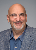
Eduardo de la Torre (Also: Tutorial Speaker)
Universidad Politécnica de Madrid (Spain)
Topic: Towards Smarter Reconfigurable Systems
Abstract: End users of electronic products demand not only more performant systems, but also to be lower energy consuming and more trustable and durable than ever. Durability refers to two aspects: on one side, products are expected to be robust enough so they can operate without problems for long periods of time, without visible malfunction and, on the other side, flexible enough so they may react to changing operational conditions, including environmental changes, functional changes or system changes (wear out, occurrence of faults, etc).
Traditionally, hardware systems offer good performance and, compared to software-based systems, low energy consumption. However, they are not as flexible as software. So, how to combine both aspects? Reconfigurable systems offer an intermediate solution with hardware-equivalent performance and software-equivalent flexibility. Even under the consideration of reconfigurable systems, flexibility and smartness are not easy to achieve. To guarantee adaptiveness, of even better, self-adaptiveness, adaptiveness, several of the so called self-* features, such as self-reconfiguration, self-calibration, self-protection, self-awareness or even self-repair, are able to provide this referred smartness.
This talk provides a general overview on the benefits of using FPGA-based reconfigurable systems, some application examples and, later on, it goes deeper on how these systems may contribute to higher adaptiveness and smartness. Later, a classification of autonomy levels is presented. In the second part of the talk, two example systems are presented. First, a reconfigurable architecture to dynamically trade-off between performance, fault tolerance and energy consumption is shown, demonstrating how systems may adapt to changing execution conditions. Second, an evolvable hardware system, able of self-adapting to changing functionality and even self-healing from faults, is presented.
Bio: Eduardo de la Torre is an Associate Professor of Electronics since 2002, and obtained his MSC and PhD degrees in Electrical Engineering from UPM in 1989 and 2000, respectively. His main expertise is in FPGA-based design and, in particular, on partial and dynamic reconfiguration of digital systems and emulation platforms for digital communications. He has more than 40 papers on reconfigurable systems in the last five years, and he is or has been Program Co-Chair of Reconfig (2012 and 2013), DASIP (20123) and SPIE VLSI Circuits & Systems (2009 and 2011) Conferences, as well as Program Committee member of Conferences such as FPL, ReCoSoC, RAW, WRC, ISVLSI, SIES. He is also reviewer of numerous Conferences and Journals such as IEEE Transactions on Computers, IEEE Transactions on Industrial Informatics, IEEE Transactions on Industrial Electronics, Sensor Magazine.ork security and privacy.
Tutorial Speakers
Rajeev Ranjan (Also: Invited Speaker)
Cadence Design System, Inc. (USA)
Topic: Accelerating SoC Design and Verification with Formal Technology
Abstract: Over the last decade, formal verification technology has made significant impact in bringing quality and productivity gains in SoC design and verification flow – ranging from architectural modeling to RTL development to SoC integration all the way to post-silicon debugging. Today, a variety of targeted verification tasks, e.g. register verification, x-propagation verification, connectivity verification, etc. can be performed solely by formal verification technology without depending on a complementary simulation flow. Verifying security attributes of an SoC is emerging as a challenging area as the IoT era dawns upon us. While the security risks in a system pertain to potential flaws in both hardware and software components, establishing hardware security is critical, because it forms the foundation for secure applications and a security hole in hardware implementation can compromise the entire system.
In this talk, we will first provide a brief overview of formal technology and its applications, followed by a broader discussion on the scalable methods of applying formal technology for hardware security verification.
Bio: Rajeev Ranjan is leading the business development efforts of a newly formed business unit at Cadence following the acquisition of Jasper Design Automation, where he was the CTO and was responsible for developing Jasper’s overall technology vision and driving the business value of formal.
Rajeev has been active in the area of formal verification for over 20 years. He has served in the organization and program committee of many international conferences including DAC, ICCAD, FMCAD, and CHARME. He has published numerous articles and has 12 patents in the area of functional verification. Rajeev received his Bachelor’s degree from Indian Institute of Technology, Kanpur (aka IIT Kanpur), his Master’s degree from University of Illinois at Urbana-Champaign (aka UIUC), and his doctorate degree from University of California at Berkeley (aka UC Berkeley). He also has an MBA degree from Wharton School of Business with a focus on entrepreneurial management and finance.
 Reinhart Job
University of Applied Sciences Muenster (Germany)
Topic: Development Process for MEMS Pressure Sensors with CMOS Read-Out Circuitry
Abstract: Devices with a combination of mechanical and electrical functionality are called ‘Micro-Electro- Mechanical Systems’ (MEMS). In case of piezoresistive MEMS pressure sensors, the mechanical deflection of a silicon membrane under pressure load results in a resistivity change of the implanted resistors. This resistivity change is then amplified and conditioned by a subsequent electrical circuitry.
Today, there is a rising demand for pressure sensors in automotive, industrial and medical applications.
Pressure sensors are designed to their dedicated application, and there are no standard sensor devices for many different applications on the market. As a consequence, a lot of different silicon based piezoresistive pressure sensors are on the market.
Monolithic integrated pressure sensor systems are realized by the combination of the two different technologies: CMOS-technology for the electrical part and MEMS-technology for the pressure sensor part. The challenge here is to design the pressure sensor cell in such a way that a wide pressure range can be covered with one fix lateral membrane size, as any change in this lateral dimensions would lead to a new CMOS design, resulting in high costs.
The detailed knowledge of the generation of the electrical signal of the sensor, and the knowledge of the effect of production process deviations on the characteristics and performance of a sensor is a key for a design of a wide range of applications.
The paper exemplarily describes the approach how to realize such a pressure sensor system to be able on one hand to measure a nominal pressure range of several bar, but also to measure the low pressure range of several tenth of mbar by keeping a sufficient signal to noise ratio, and without changing the original CMOS circuitry. Further on, the influence of certain process deviations is investigated, and the mechanical stability of the membrane concerning pressure overload as an important specification parameter is considered. A method will be presented that allows calculating the electrical signals of Wheatstone-Bridge based silicon pressure sensors, using general semiconductor fundamentals from the theory of piezoresistivity. The effect of different implant profiles and certain production process deviations during the fabrication of the membrane (e.g. membrane thickness deviations) are considered.
For the calculation of the sensor signal, an analytical approach, based on the theory of piezoresistivity, is combined it with structural mechanical simulation of mechanical stress, utilizing the Finite Element Analysis (FEA). A comparison between theoretical signal evaluation and measurement as a proof of feasibility of the approach is given.
As the requirements of the performance of pressure sensors are increasing by the rapidly growing applications strictly defined procedures during development and production, which confine the options of possible solutions, have to be followed. An investigation of potential failure modes and a systematically development flow of new sensors, also considering the application, as described in the ISO 26262 standard, is mandatory if the application of the sensor is rated as functional safety related.
Bio: Reinhart Job studied physics at the University of Bochum, Germany, and received his doctorate in experimental solid state physics. For 17 years he worked at the Open University in Hagen, first as a scientist, and after his habilitation in the field of technology of electronic components, as a professor. Since 2011 he is with the University of Applied Sciences Muenster, where he acts since 2013 as dean of the Faculty of Electrical Engineering and Computer Science. Reinhart Job authored and co-authored more than 200 publications on Applied Solid State Physics and semiconductor materials research for international journals.
 Eduardo de la Torre (Also: Invited Speaker)
Universidad Politécnica de Madrid (Spain)
Topic: Partial Reconfiguration Applied to Dynamic Multithread Hardware Acceleration and Evolvable Hardware
Abstract: Although partial reconfiguration in FPGAs is theoretically as easy as writing new contents in the configuration memory, the questions on what, when, and how to reconfigure the FPGA may make this task not that easy. The situation may be worse if these questions are merged with an even more important question: what for?
In this tutorial, the basics on partial reconfiguration using position-independent bitstreams are shown. After a brief FPGA internal architecture description (centered on series 7 Xilinx devices), the correspondence between addresses in the configuration memory and its equivalent positions in the reconfigurable fabric are shown. Reconfiguration with position reallocation is introduced afterwards. This solves, in some manner, the question on ‘how’ to reconfigure.
As an application example (trying to partially answer the ‘what for’ question), we present a multi-slot architecture, called Artico3, which allows dynamic execution of multiple threads by using a variable set of HW accelerators, obtained by means of a High Level Synthesis process (i.e., answering ‘what’ to reconfigure),. The architecture is suited for, dynamically at runtime, trading performance versus fault tolerance and energy consumption. A task scheduler decides, at runtime, ‘when’ and ‘what’ accelerators are to be run, according to possibly changing system requirements. A live demo will be provided, showing this architecture running in different performance/fault tolerance/energy consumption operation points, moving from one mode into another by means of dynamic and partial reconfiguration.
As a second application, an evolvable HW platform is presented. In this case, HW is created autonomously, according to changes proposed by an evolutionary algorithm. During evolution, circuit functionality is improved by checking circuit quality, defined by a fitness function which sets the optimization criteria to follow. In this sense, circuits are automatically generated by combining small building blocks (tiny processing elements) into an array structure, whose contents are decided autonomously by evolutionary rules. Every iteration requires new circuits to be generated by using partial reconfiguration.
A live demo will also be provided in this case, with an image processing/filtering application which gathers many properties of evolvable HW. Optimized reconfiguration engines allow over 100,000 circuit evaluations/second, with high processing speeds over 400 Mpixels/second. Also, the fact of self-evolving on the reconfigurable array provides self-healing capabilities, which will be shown in the demo by means of artificially injecting faults on the array, and observing how the system reacts to circumvent these faults.
Bio: Eduardo de la Torre is an Associate Professor of Electronics since 2002, and obtained his MSC and PhD degrees in Electrical Engineering from UPM in 1989 and 2000, respectively. His main expertise is in FPGA-based design and, in particular, on partial and dynamic reconfiguration of digital systems and emulation platforms for digital communications. He has more than 40 papers on reconfigurable systems in the last five years, and he is or has been Program Co-Chair of Reconfig (2012 and 2013), DASIP (20123) and SPIE VLSI Circuits & Systems (2009 and 2011) Conferences, as well as Program Committee member of Conferences such as FPL, ReCoSoC, RAW, WRC, ISVLSI, SIES. He is also reviewer of numerous Conferences and Journals such as IEEE Transactions on Computers, IEEE Transactions on Industrial Informatics, IEEE Transactions on Industrial Electronics, Sensor Magazine.ork security and privacy.
 Bertrand Saillet
Unitec Semicondutores
Topic: Yield learning of CMOS technology during development and mass production
Abstract: Yield is defined as the number of products that can be sold relative to the number of products started. Yield is a quality metric, and high Yield is a major goal of semiconductor operations as it directly impact costs. Semiconductor operations use to monitor and enhance line yields and die yields. The tutorial will focus on die yields, defined as the number of good dice passing wafer probe testing from wafers that reach that part of the process. It will describe how product achievable yields are being evaluated and how yields are improved over time from early development to mass production.
Bio: Bertrand Saillet is Technology Integrator at Unitec Semicondutores, a Brazilian company developing Integrated Circuits and owning the largest and most modern semiconductor fab in the southern hemisphere. Before joining Unitec, he developed, introduced, and managed a large number of technologies and products into semiconductor fabs by working at LFoundry as Yield and Process Integration manager from 2010 to 2014, Atmel as Yield manager from 2006 to 2010 and previously ST Microelectronics as research engineer. Mr Saillet is a Microelectronics and Telecommunication engineer graduated from Polytech’ Marseille and received a Master degree in Nano-electronics and Science Engineering from Aix-Marseille University in France.
 Shishpal Rawat
Intel Corporation (USA)
Accellera Systems Initiative Chair
Topic: IEEE/CEDA
Abstract: TBD
Bio: Mr. Shishpal Rawat has been the Chairman of the Board at Accellera Organization Inc. since July 2010. Mr. Rawat served as a Director of EDA Investments and ArchPro Design Automation, Inc. He serves as a Director of Business Enabling Programs with the Design Technology Solutions group, Intel. He has been at Intel for 22 years and has held a variety of Design and CAD management positions. He holds M.S. and Ph.D. degrees in Computer Science from Pennsylvania State University, University Park, and a B.Tech. degree in Electrical Engineering from Indian Institute of Technology, Kanpur, India.


