Tutorials*
*All SBMICRO Tutorials are sponsored by IEEE/Electron Device Society – 2022 EDS Brazil Mini-colloquium
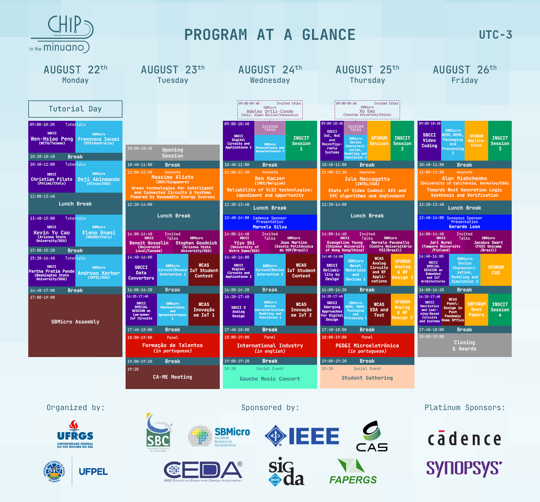
August 22th
09:00 – 10:20 – SBMicro Tutorial – Augmenting silicon technologies with graphene
Francesca Iacopi (University of Technology Sidney, Australia)
Location: SBMicro Cadence Auditorium
Chair: Michelly de Souza (FEI, Brazil)
ABSTRACT: Harnessing graphene’s properties on a silicon platform could augment integrated technologies with a broad range of novel miniaturized functionalities. We will review the learnings from the development of our epitaxial graphene on silicon carbide on silicon technology and some of its most promising applications. This platform allows to obtain any complex graphene -coated silicon carbide 3D nanostructures in a site – selective fashion at the wafer -scale and with sufficient adhesion for integration. Key capabilities for nano-optics and metasurfaces in the MIR are specifically unlocked by the graphene/silicon carbide combination. We have recently demonstrated that the sheet resistance of epitaxial graphene on 3C-SiC on silicon is comparable to that of epitaxial graphene on SiC wafers, despite substantially smaller grains. We also indicate that the control of the graphene interfaces, particularly when integrated, can be a more important factor than achieving large grain sizes. In addition, we show that well- engineered defects in graphene are preferable to defect -free graphene for most electrochemical applications, including biosensing. Promising examples of application of this technology in the More than Moore domain include integrated energy storage, MIR sensing and detection, and sensors for electro-encephalography.
BIO: Francesca Iacopi received her MSc in Physics from Roma La Sapienza University, Italy (1996), her PhD in E.E./Materials Science from the Katholieke Universiteit Leuven, Belgium (2004), and she is currently Professor of Nanoelectronics, in the Faculty of Engineering and IT of the University of Technology Sydney, and Chief Investigator of the ARC Centre of Excellence in Transformative Meta-Optical Systems (TMOS). Iacopi has over 20 years’ R&D experience in semiconductor Industry and Academia. Her research focus is the translation of basic scientific advances in nanomaterials and novel device concepts into industrial processes. Her seminal work at IMEC on low-k dielectrics for on-chip interconnects over the 1999-2009 decade has informed the industrial uptake of porous dielectrics into modern semiconductor microprocessors. More recently, she invented a process to harness the properties of graphene on silicon for integrated micro-technologies. Major awards include a Gold Graduate Student Award from the Materials Research Society (2003), a Future Fellowship from the Australian Research Council (2012-2016), a Global Innovation Award (TechConnect, 2014) and was listed among the 30 most innovative Australian engineers in 2018. Prof. Iacopi is a Fellow of the Institute of Engineers Australia, serves in the Board of Governors of IEEE EDS (2021-23), as well as in various technical and strategic committees for IEEE and the Materials Research Society, and was selected as EDS Distinguished Lecturer in 2021.
09:00 – 10:20 – SBCCI Tutorial – Recent Advances in Learning-based Image and Video Coding
Wen Hsiao Peng (NCTU, Taiwan)
Location: SBCCI Synopsys Auditorium
Chair: Arthur Lorenzon (UFRGS, Brazil)
ABSTRACT: Digital image/video coding has been widely used in our daily life products. Nowadays, nearly every video-enabled device has image/video coding modules. In the past 30 years, several series of international image/video coding standards have been developed and adopted by industry. Recently, learning-based image/video coding, particularly end-to-end learned image/video coding, shows great promise in many emerging applications, e.g. perceptual compression for realism and application-specific image/video compression. This fast growing sector has attracted more than 100+ publications in the literature, with the state-of-the-art end-to-end learned image coding showing comparable compression performance to H.266/VVC intra coding in terms of PSNR and much better MS-SSIM results. End-to-end learned video coding is also catching up quickly. Some preliminary studies report comparable PSNR results to H.265/HEVC or even H.266/VVC under the low-delay setting. These interesting results have led to intense activity in international standards organizations (e.g. JPEG AI) and various Challenges (e.g. CLIC at CVPR and Grand Challenge on Neural Network-based Video Coding at ISCAS). This talk shall give an overview of this field, introducing some notable systems and recent breakthroughs. Furthermore, it shall disclose research opportunities related to the hidden aspects of this new technology.
BIO: Dr. Wen-Hsiao Peng (M’09-SM’13) received his Ph.D. degree from National Chiao Tung University (NCTU), Taiwan, in 2005. He was with the Intel Microprocessor Research Laboratory, USA, from 2000 to 2001, where he was involved in the development of ISO/IEC MPEG-4 fine granularity scalability. Since 2003, he has actively participated in the ISO/IEC and ITU-T video coding standardization process and contributed to the development of SVC, HEVC, and SCC standards. He was a Visiting Scholar with the IBM Thomas J. Watson Research Center, USA, from 2015 to 2016. He is currently a Professor with the Computer Science Department, National Yang Ming Chiao Tung University, Taiwan. He has authored over 75+ journal/conference papers and over 60 ISO/IEC and ITU-T standards contributions. His research interests include learning-based video/image compression, deep/machine learning, multimedia analytics, and computer vision. Dr. Peng was Chair of the IEEE Circuits and Systems Society (CASS) Visual Signal Processing (VSPC) Technical Committee. He was Technical Program Co-chair for 2021 IEEE VCIP, 2011 IEEE VCIP, 2017 IEEE ISPACS, and 2018 APSIPA ASC; Publication Chair for 2019 IEEE ICIP; Area Chair/Session Chair/Tutorial Speaker/Special Session Organizer for IEEE ICME, IEEE VCIP, and APSIPA ASC; and Track/Session Chair and Review Committee Member for IEEE ISCAS. He served as AEiC for Digital Communications for IEEE JETCAS and Associate Editor for IEEE TCSVT. He was Lead Guest Editor, Guest Editor and SEB Member for IEEE JETCAS, and Guest Editor for IEEE TCAS-II. He was Distinguished Lecturer of APSIPA and the IEEE CASS.
10:40 – 12:00 – SBMicro Tutorial – New Applications of 2D Materials from Wearable Health to Memory Devices and 5G Switches
Deji Akinwande (UTexas, USA)
Location: SBMicro Cadence Auditorium
Chair: Stanislav Mochkalev (Unicamp, Brazil)

ABSTRACT: This talk will present our latest research adventures on 2D nanomaterials towards greater scientific understanding and advanced engineering applications. In particular, the talk will highlight our work on flexible electronics, zero-power devices, single-atom monolayer memory, non-volatile RF/5G/6G switches, and wearable tattoo sensors for mobile health. Non-volatile memory devices based on 2D materials are an application of defects and is a rapidly advancing field with rich physics that can be attributed to metal adsorption into vacancies. The memory devices can be used for neuromorphic computing and operate as switches up to 500GHz. Likewise, from a practical point, electronic tattoos based on graphene have ushered a new material platform that has highly desirable practical attributes including optical transparency, mechanical imperceptibility, and is the thinnest conductive electrode sensor that can be integrated on skin for physiological measurements including blood pressure monitoring with Class A performance. Much of these research achievements have been published in leading journals.
BIO: Deji Akinwande is an Endowed Full Professor at the University of Texas at Austin, and a Fellow of the IEEE and APS. He received the PhD degree from Stanford University in 2009. His research focuses on 2D materials and nanoelectronics/technology, pioneering device innovations from lab towards applications. Prof. Akinwande has been honored with the 2019 Fulbright Specialist Award, 2017 Bessel-Humboldt Research Award, the U.S Presidential PECASE award, the inaugural Gordon Moore Inventor Fellow award, the inaugural IEEE Nano Geim and Novoselov Graphene Prize, the IEEE “Early Career Award” in Nanotechnology, the NSF CAREER award, several DoD Young Investigator awards, and was a past recipient of fellowships from the Kilby/TI, Ford Foundation, Alfred P. Sloan Foundation, 3M, and Stanford DARE Initiative. His research achievements have been featured by Nature news, Time and Forbes magazine, BBC, Discover magazine, Wall Street Journal, and many media outlets. He serves as an Editor for the IEEE Electron Device Letters and Nature NPJ 2D Materials and Applications. He Chairs the 2022 Gordon Research Conference on 2D materials, and was the past chair of the 2019 Device Research Conference (DRC), and the 2018 Nano-device committee of IEEE IEDM Conference.
10:40 – 12:00 – SBCCI Tutorial – Electronic system-level design for hardware IP protection
Christian Pilato (POLIMI, Italy)
Location: SBCCI Synopsys Auditorium
Chair: Gabriel Nazar (UFRGS, Brazil)
ABSTRACT: The globalization of the electronics supply chain allows for the reduction of chip manufacturing costs but poses new security threats. Untrusted foundries can steal the intellectual property in the chips, while malicious users can tamper with the systems to harm their execution, steal sensitive information, or support reverse engineering. The design of next-generation systems demands the introduction of such security concepts at higher levels of abstraction. In this tutorial, I will present an overview of the security concerns in the design of heterogeneous system-on-chip architectures. I will also discuss how traditional methods for electronic system-level design can be extended to design and prototype architectures with secure communications, to automatically synthesize security countermeasures, and to protect existing IP hardware modules.
BIO: Christian Pilato is a Tenure-Track Assistant Professor at Politecnico di Milano. He was a Post-doc Research Scientist at Columbia University (2013-2016) and at the ALaRI Institute of the Università della Svizzera italiana (2016-2018). He was also a Visiting Researcher at New York University, Delft University of Technology, and Chalmers University of Technology. He has a Ph.D. in Information Technology from Politecnico di Milano (2011). His research interests focus on the design, optimization, and prototyping of heterogeneous system-on-chip architectures and reconfigurable systems, with emphasis on memory and security aspects. Starting from October 2020, he is the Scientific Coordinator of the H2020 EVEREST project. He served as program chair of EUC 2014 and will be the program chair of ICCD 2022. He is also serving in the program committees of many conferences on EDA, CAD, embedded systems, and reconfigurable architectures (DAC, ICCAD, DATE, CASES, ASPDAC, FPL, ICCD, etc.) He is a Senior Member of IEEE and ACM, and a Member of HiPEAC.
13:40 – 15:00 – SBMicro Tutorial – Trends and challenges in Nanoelectronics for the next decade
Elena Gnani (Unibo, Italy)
Location: SBMicro Cadence Auditorium
Chair: Renan Trevisoli (PUC-SP/UFABC, Brazil)
ABSTRACT: In the last decade nanoelectronics devices have been a driving force for societal applications and for a greensustainable world. Key fields such as security, energy, healthcare, transport, communication and infotainment aregaining more and more market so that microelectronics is becoming an inherent part of everyday life. The researchrelated to nanoelectronics can be grouped in three main directions, i.e., More Moore, Beyond CMOS and Morethan Moore. General trends and challenges will be addressed.
BIO: Elena Gnani is Associate Professor at the University of Bologna. Her research interests include the developmentof physical transport models in semiconductor devices and numerical-analysis techniques, with special emphasison the study of quantum-confined devices, such as FinFETs, silicon nanowires (NW), steep-slope devices as wellas quasi ballistic transport in nanoMOSFETs. E. Gnani is author or co-author of more than 180 papers published inreferred international journals and in proceedings of major international conferences. She is presently an IEEESenior Member, EDS Distinguished, member of the EDS Technology Computer Aided Design Committee andserves as an associate editor of the IEEE Transactions on Electron Devices.
13:40 – 15:00 – SBCCI Tutorial – Reliable In-memory Computing with Unreliable Devices and Circuits
Kevin Yu Cao (Arizona State University, USA)
Location: SBCCI Synopsys Auditorium
Chair: José Augusto Nacif (UFV, Brazil)
ABSTRACT: With the ever-increasing demand of AI algorithms and high-definition sensors, Contemporary microprocessor design is facing tremendous challenges in memory bandwidth, processing speed and power consumption. Leveraging the advances in device technology and design techniques, in-memory computing (IMC) embeds analog deep-learning operations in the memory array, achieving massively parallel computing with high storage density. On the other side, its performance is still limited by device non-idealities, circuit precision, on-chip interconnection, and algorithm properties. In this talk, we will first review the state-of-the-art IMC design techniques, such as those based on resistive random-access memory (RRAM) and SRAM. Then based on statistical data from a fully integrated 65nm CMOS/RRAM test chip, we will illustrate the bottlenecks of current IMC system, including RRAM variations, the stability of machine learning models, peripheral circuits and interconnection. They interact with each other, limiting the inference accuracy and system energy-delay product (EDP). To efficiently explore design space, we will present a newly developed benchmark simulator, SIAM, which integrates device, circuit, architecture, network-on-chip (NoC), network-on-package (NoP) and DRAM access models to address the bottlenecks in data movement and robustness. Furthermore, we will demonstrate two methods to recover the accuracy loss: training for model stability before mapping to the hardware, and a hybrid SRAM/RRAM architecture for post-mapping recovery. These methods are applied to various datasets as well as a 65nm SRAM/RRAM test chip, helping shed light on future IMC research focus.
BIO: Yu Cao received the B.S. degree in physics from Peking University in 1996. He received the M.A. degree in biophysics and the Ph.D. degree in electrical engineering from University of California, Berkeley, in 1999 and 2002, respectively. He is now a Professor of Electrical Engineering at Arizona State University, Tempe, Arizona. He has published numerous articles and two books on nano-CMOS modeling and physical design. His research interests include neural-inspired computing, hardware design for on-chip learning, and reliable integration of nanoelectronics. Dr. Cao is a Distinguished Lecturer of the IEEE Circuits and Systems Society. He was a recipient of the 2020 Intel Outstanding Researcher Award, the 2009 ACM SIGDA Outstanding New Faculty Award, the 2006 NSF CAREER Award, the 2006 and 2007 IBM Faculty Award, and five Best Paper Awards. He is a Fellow of the IEEE.
15:20 – 16:40 – SBMicro Tutorial – Reliability of Metal Gate / High-K CMOS devices
Andreas Kerber (INTEL, USA)
Location: SBMicro Cadence Auditorium
Chair: Rodrigo Trevisoli Doria (FEI, Brazil)
ABSTRACT: Aggressively scaled transistor technologies with metal gate/high-k stacks encounter additional reliability challenges beside bias temperature instability (BTI) in PMOS and NMOS devices, time dependent dielectric breakdown and hot carrier degradation. Time-zero variability and variability induced by device aging is a growing concern which needs to be modeled using stochastic processes. The physical nature of the stochastic process remains under debate and to support model development efforts large statistical data sets are essential. In addition, self-heating during reliability testing can be observed in novel device structures like bulk FinFET, SOI FinFETs, FDSOI and gate-all-around devices and needs proper attention. Furthermore, to increase the confidence in the discrete device reliability models, device-to-circuit correlations need to be established. In this presentation we discuss how to obtain stochastic BTI data for discrete SRAM and logic device beyond 3sigma, address device-to-circuit correlations using ring-oscillators and explore self-heating effects in FinFET and SOI devices.
BIO: Andreas Kerber received his Diploma in physics from the University of Innsbruck, Austria, in 2001, and a PhD in electrical engineering from the TU-Darmstadt, Germany, with honors in 2014. From 1999 to 2000 he was an intern at Bell Laboratories, Lucent Technologies (Murray Hill, NJ, USA) working on the electrical characterization of ultra-thin gate oxides. From 2001 to 2003, he was the Infineon Technologies assignee to International SEMATECH at IMEC in Leuven, Belgium, where he was involved in the electrical characterization of alternative gate dielectrics for sub-100 nm CMOS technologies. From 2004 to 2006, he was with the Reliability Methodology Department at Infineon Technologies in Munich, Germany, responsible for the dielectric reliability qualification of process technology transfers of 110 and 90 nm memory products. During that time he developed a low-cost, fast wafer-level data acquisition setup for time-dependent dielectric breakdown (TDDB) testing with sub-ms time resolution. From 2006 to 2018 he was working for AMD in Yorktown Heights, NY, and GLOBALFOUNDRIES in Malta and East-Fishkill, NY, as a Principal Member of Technical Staff on front-end-of-line (FEOL) reliability research with focus on metal gate / high-k CMOS process technology, advanced transistor architecture and device-to-circuit reliability correlation. From 2018 to 2019 he was with Skorpios Technologies in Albuquerque, NM, working on reliability of Si-photonic devices. From Nov. 2019 to March 2021 he was with ON-Semiconductor in Santa Clara, CA working on product quality management of CMOS image sensors for automotive, consumer and industrial markets. Since March 2021 he is with Intel in Santa Clara, CA working on CMOS reliability for 3D-NAND technology. Dr. Kerber has contributed to more than 110 journal and conference publications and presented his work at international conferences, including the IEDM, VLSI and IRPS. In addition, he has presented tutorials on metal gate / high-k reliability characterization at the IIRW, IRPS and ICMTS. Dr. Kerber has served as a technical program committee member for the SISC, IRPS, IIRW, IEDM, Infos, ESSDERC, is a Senior Member of the IEEE and a Distinguished Lecturer (DL) for the IEEE Electron Devices Society.
15:20 – 16:40 – SBCCI Tutorial – Interconnect Meets Architecture: On-Chip Communication in the Age of Heterogeneity
Partha Pratim Pande (Washington State University, USA)
Location: SBCCI Synopsys Auditorium
Chair: Mateus Rutzig (UFSM, Brazil)
ABSTRACT: Neural Networks, graph analytics, and other big-data applications have become vastly important for many domains. This has led to a search for proper computing systems that can efficiently utilize the tremendous amount of data parallelism that is associated with these applications. Generally, we depend on data centers and high-performance computing (HPC) clusters to run various big-data applications. However, the design of data centers is dominated by power, thermal, and physical constraints. On the contrary, emerging heterogeneous manycore processing platforms that consist of CPU and GPU cores along with memory controllers (MCs) and accelerators have small footprints. Moreover, they offer power and area-efficient tradeoffs for running big-data applications. Consequently, heterogeneous manycore computing platforms represent a powerful alternative to the data center-oriented type of computing. However, typical Network-On-Chip (NoC) infrastructures employed on conventional manycore platforms are highly sub-optimal to handle specific needs CPUs, GPUs, and accelerators. To address this challenge, we need to come up with a holistic approach to design an optimal network-on-chip (NoC) as the interconnection backbone for the heterogeneous manycore platforms that can handle CPU, GPU, and application-specific accelerator communication requirements efficiently. We will discuss design of a hybrid NoC architecture suitable for heterogeneous manycore platforms. We will also highlight effectiveness of machine learning-inspired multi-objective optimization (MOO) algorithms to quickly find a NoC that satisfies both CPU and GPU communication requirements. Widely used MOO techniques (e.g., NSGA-II or simulated annealing based AMOSA) can require significant amounts of time due to their exploratory nature. Therefore, more efficient, and scalable ML-based optimization techniques are required. We are going to discuss various features of a generalized application-agnostic heterogeneous NoC design that achieves similar levels of performance (latency, throughput, energy, and temperature) as application-specific designs. In this talk, we will first review the state-of-the-art IMC design techniques, such as those based on resistive random-access memory (RRAM) and SRAM. Then based on statistical data from a fully integrated 65nm CMOS/RRAM test chip, we will illustrate the bottlenecks of current IMC system, including RRAM variations, the stability of machine learning models, peripheral circuits and interconnection. They interact with each other, limiting the inference accuracy and system energy-delay product (EDP). To efficiently explore design space, we will present a newly developed benchmark simulator, SIAM, which integrates device, circuit, architecture, network-on-chip (NoC), network-on-package (NoP) and DRAM access models to address the bottlenecks in data movement and robustness. Furthermore, we will demonstrate two methods to recover the accuracy loss: training for model stability before mapping to the hardware, and a hybrid SRAM/RRAM architecture for post-mapping recovery. These methods are applied to various datasets as well as a 65nm SRAM/RRAM test chip, helping shed light on future IMC research focus.
BIO: Partha Pratim Pande is a professor and holder of the Boeing Centennial Chair in computer engineering at the school of Electrical Engineering and Computer Science, Washington State University, Pullman, USA. He is currently the director of the school. His current research interests are novel interconnect architectures for manycore chips, on-chip wireless communication networks, heterogeneous architectures, and ML for EDA. Dr. Pande currently serves as the Editor-in-Chief (EIC) of IEEE Design and Test (D&T). He is on the editorial boards of IEEE Transactions on VLSI (TVLSI) and ACM Journal of Emerging Technologies in Computing Systems (JETC) and IEEE Embedded Systems letters. He was/is the technical program committee chair of IEEE/ACM Network-on-Chip Symposium 2015 and CASES (2019-2020). He also serves on the program committees of many reputed international conferences. He has won the NSF CAREER award in 2009. He is the winner of the Anjan Bose outstanding researcher award from the college of engineering, Washington State University in 2013. He is a fellow of IEEE.
KEYNOTES
August 23th
11:00 – 12:20 – KEYNOTE – Green Technologies for Intelligent and Connected Circuits & Systems Powered by Renewable Energy Sources
Massimo Alioto (NUS, Singapore)
Location: SBCCI Synopsys Auditorium
Chair: Nuno Roma (IST, Portugal)
ABSTRACT: The growth in the number of connected devices towards the trillion scale will be fundamentally impeded by batteries as a conventional source of energy, as their deployment in the trillions poses clear economic, logistical and environmental sustainability challenges.
This keynote introduces the key ideas and their silicon demonstrations to enable a new breed of always-on silicon systems from sensing, to computing and wireless communications with no battery inside (or any other energy storage). Sensor interfaces, processors and wireless transceivers fitting existing infrastructure (e.g., WiFi) with power reductions by orders of magnitude are discussed and exemplified by recent silicon demonstrations, and their system integration.
Ultimately, the technological pathway discussed in this keynote supports sustainable growth of applications leveraging large-scale deployments of silicon systems, making our planet smarter. And greener too.
BIO: Massimo Alioto (Fellow, IEEE) is currently a Professor with the Department of Electrical and Computer Engineering, National University of Singapore, Singapore, where he leads the Green IC Group, and also the Director of the Integrated Circuits and Embedded Systems Area and the FD-FAbrICS research center on intelligent&connected systems. Previously, he held positions at the University of Siena (Italy), Intel Labs (USA), University of Michigan, Ann Arbor (USA), University of California at Berkeley (USA), and EPFL (Switzerland).
He has authored or coauthored about 350 publications on journals and conference proceedings. He is the coauthor of five books printed by Springer, including the popular Enabling the Internet of Things—From Circuits to Systems (Springer, 2017). His research interests include self-powered integrated systems, intelligent and connected systems, widely energy-scalable integrated systems, data-driven systems for edge computing, hardware security, and emerging technologies.
Prof. Alioto is the Editor-in-Chief of IEEE Transactions on Very Large Scale Integration (VLSI) Systems, and is/was a Distinguished Lecturer of the IEEE Solid-State Circuits and Circuits and Systems Society, for which he was also a member of the Board of Governors. He is/was the Technical Program Chair (e.g., ISCAS 2023, SOCC, ICECS, and NEWCAS) in numerous conferences, and is in the IEEE “Digital Architectures and Systems” ISSCC Subcommittee and the IEEE ASSCC TPC. He has served as a Guest Editor for several IEEE journal special issues (e.g., JSSC, TCAS-I, TCAS-II, JETCAS) and an Associate Editor for a number of IEEE and ACM journals. He was the Deputy Editor-in-Chief of IEEE Journal on Emerging and Selected Topics in Circuits and Systems. Prof. Alioto is an IEEE Fellow.
August 24th
11:00 – 12:20 – KEYNOTE – Reliability of VLSI technologies: impediment and opportunity
Ben Kaczer (IMEC, Belgium)
Location: SBMicro Cadence Auditorium
Chair: Gilson Wirth (UFRGS, Brazil)
ABSTRACT: Presence of non-idealities and defects in VLSI technologies is an immutable reality, which, however, is often overlooked by device engineers, researchers, technologists, and designers alike. We argue that in fact VLSI reliability “makes or breaks” any new technology. Superficial device reliability optimization is possible using phenomenological observations only, but we argue that solid physical foundations and thorough understanding of the underlying degradation mechanisms are essential both for truly dependable lifetime projections and for novel device pathfinding. Based on the detailed investigation of gate oxide defects, our “defect engineering” approach enables, among other things, optimization paths for SiGe channel devices and new oxidation techniques for advanced gate-all-around architectures, such as nanosheets and forksheets. In deeply scaled devices, degradation mechanisms can be decomposed down to individual defects, with each defect measured separately and its properties described down to single Kelvin temperatures using quantum mechanics. Such knowledge then allows us e.g. to model the degradation statistics of deeply-scaled devices and to predict the likelihoods of their failure. Robust degradation models enable us to project wider safe operating areas, which in turn allow to design better-performing circuitry at a given technology node and thus limited costs. Moreover, the ubiquitous presence of defects can be in fact embraced and the in-depth knowledge of defect properties can be used to our advantage to design new devices and applications, ranging from memory to physically unclonable functions and tamper-aware aging monitors.
BIO: Dr. Ben Kaczer is a Scientific Director in the FEOL reliability group at imec. Dr. Kaczer received the M.S. degree in Physical Electronics from Charles University, Prague, in 1992 and the M.S. and Ph.D. degrees in Physics from The Ohio State University, in 1996 and 1998, respectively. For his Ph.D. research on the ballistic-electron emission microscopy of SiO2 and SiC films he received the OSU Presidential Fellowship and support from Texas Instruments, Inc. In 1998 he joined the reliability group of imec, Leuven, Belgium, where his activities have included the research of the degradation phenomena and reliability assessment of SiO2, SiON, high-k, and ferroelectric films, planar and multiple-gate FETs, circuits, and characterization of Ge, SiGe, III-V, and MIM devices.
He has co-authored more than 500 journal and conference papers and 4 patent groups related to device and circuit reliability, presented a number of invited papers and tutorials, and received 6 IEEE International Reliability Physics Symposium (IRPS) Best and Outstanding Paper Awards, 2 IEEE IPFA Best Paper Awards, and the 2011 IEEE EDS Paul Rappaport Award. In 2019 he was historically the most cited author of IRPS. His h-index on Google Scholar is 62.
Dr. Kaczer has served twice as the chair of the Characterization, Reliability and Yield subcommittee of the International Electron Device Meeting (IEDM; 2007 and 2015) and as a member of various subcommittees of the IRPS (2002—2016) and is currently serving as a member of IRPS management committee (2018—). He was the General Chair of the Semiconductor Interfaces Specialists Conference (SISC; 2006) and continues to act as the conference secretary (2007—). He co-organized the INFOS conference (2005), and served on the INFOS, WoDiM, IPFA, and ICICDT conference committees. He has served on the Editorial Board of IEEE journal of Transaction of Electron Devices for three terms (2011—2019).
August 25th
11:00 – 12:20 – KEYNOTE – State of Video Codecs: AV1 and VVC algorithms and deployment
Iole Moccagatta (INTEL, USA)
Location: SBCCI Synopsys Auditorium
Chair: Bruno Zatt (UFPel, Brazil)
ABSTRACT: TBD
BIO: Dr. Iole Moccagatta is a Principal Engineer at Intel working on HW Multimedia IPs that are integrated on Intel platforms. Prior to Intel she hold the position of Senior Video Architect at NVIDIA, and that of Science Director at IMEC, Belgium. Dr. Moccagatta has been a very active member of MPEG, ITU-T, and JPEG, where she has represented US interests and companies and made a large number of technical contributions. A number of those have been included in MPEG and JPEG standards. She is currently Co-chair of the MPEG/ITU-T Joint Video Experts Team (JVET) Ad-Hoc Group on H.266/VVC Conformance and Co-editor of the H.266/VVC Conformance Testing document. Dr. Moccagatta has also been an active participant of the Alliance for Open Media (AOM) AV1 Codec WG, where she has co-authored two adopted proposals. She currently represents Intel in the AOM Board. Dr. Moccagatta is also serving as IEEE Signal Processing Society (SPS) Regional Director-at-Large Regions 1-6, supporting and advising Chapters and their officers, providing input on how to serve and engage the SPS community in general, and the SPS industry members in particular, and using her professional network to attract new volunteers to serve in SPS subcommittees and task forces. Dr. Moccagatta is the author or co-author of more than 30 publications, 2 book chapters, and more than 10 talks and tutorials in the field of image and video coding. She holds more than 10 patents in the same fields. For more details see Dr. Moccagatta professional site at http://alfiole.users.sonic.net/iole/. Dr. Moccagatta received a Diploma of Electronic Engineering from the University of Pavia, Italy, and a PhD from the Swiss Federal Institute of Technology in Lausanne, Switzerland.
August 26th
11:00 – 12:20 – KEYNOTE – Towards Next Generation Logic Synthesis and Verification
Alan Mishchenko (University of California, Berkeley, USA)
Location: SBMicro Cadence Auditorium
Chair: André Reis (UFRGS, Brazil)
ABSTRACT: Given the progress achieved over the last fifty years in logic synthesis and verification, it is tempting to believe that most of the research discoveries have already been made, and the role of future researchers and engineers is just to maintain the CAD tools and occasionally make small changes, such as adding concurrency or employing machine learning to generate better scripts. Nothing could be farther from the truth. In this talk, we explore several orthogonal innovations in the fundamental research used to build synthesis tools targeting FPGAs and ASICs. These innovations include using novel data structures, leveraging synergistic optimization engines, and simultaneously exploring previously-unrelated search spaces. Most of these improvements are work-in-progress with early results demonstrating better quality and faster runtimes.
BIO: Alan graduated with M.S. from Moscow Institute of Physics and Technology (Moscow, Russia) in 1993 and received his Ph.D. from Glushkov Institute of Cybernetics (Kiev, Ukraine) in 1997. In 2002, Alan joined the EECS Department at University of California, Berkeley, where he is currently a full researcher. His research is in computationally efficient logic synthesis, formal verification, and machine learning.
SPONSOR PRESENTATIONS
August 24th
13:40 – 14:00 – SBMicro Cadence Sponsor Presentation – Cadence World class EDA solutions for IC and beyond, Growing Presence and Opportunities in Brazil.
Marcelo Silva
Location: SBMicro Cadence Auditorium
ABSTRACT: This presentation will talk about Cadence software, IP and methodologies that support the demanding requirements of IC design and the semiconductor industry. Cadence has a world-class portfolio of technologies enabling the semiconductor ecosystem with solutions based on the best in class computational algorithms and Machine Learning. Cadence’s extensive portfolio of computational software capabilities are critical in addressing the challenges associated with ever growing requirements for digital processing, analog and RF applications, and beyond. Cadence’s industry leading technologies and application of things like Machine Learning techniques, allow Cadence to continue pushing the envelope to deliver the best PPA and time to market for our customers.
BIO: Marcelo Silva received is MSEE from Federal University of Itajubá, he has 20+ years of experience on microelectronics, having started his carrier at Motorola in Jaguariuna, SP Brazil, as an analog designer in 1999, he moved to San Jose, CA, USA in 2005 where he joined Airgo, today a Qualcomm company, to work on their RF group as an Analog and Mixed Signal specialist, digital designer and verification, he then joined SiRF/CSR, joining Qualcomm, both companies based at California in Silicon valley. Returning to Brazil in 2012, Marcelo worked as design manager on CTI where he was responsible for the development of Radiation Hardened ICs design for aero special applications, he then moved to Unitec where he managed a Design Center. Recently Marcelo Silva works for Cadence Brazil in the quality of Director of Field Application Engineering team, where he is responsible for the field team covering all product lines for IC and System solutions.
August 26th
13:40 – 14:00 – SBCCI Synopsys Sponsor Presentation – Developing High Tech from Latin America to the World
Gerardo Leon
Location: SBCCI Synopsys Auditorium
ABSTRACT: Synopsys technology is at the heart of the innovation that is changing the way we live and work. Autonomous cars. Learning machines. Lightning-fast communication between billions of devices. Everything is connected. And chips are driving the new era of digital innovation. Synopsys Chile is the only Research and Development (R&D) center that Synopsys Inc. owns in Latin America. This knowledge creation center was installed in Chile in 2006, becoming a gateway to promote development and research throughout the region and thereby promote digital innovation to develop the world of the future. In this talk we will present, on the one hand, an overview of Synopsys, what we do, what the microelectronics market is, its dynamics, and how through constant innovation we enable this new era of “Smart Everything”. On the other hand, we will show how we work, profiles, career growth and development paths, along with different roles and different teams in Synopsys Chile.
BIO: Gerardo Leon is a Computer Science Engineer from the Pontificia “Universidad Catolica de Chile” with a master’s in engineering from the same university. During his career, Gerardo has been part of different research and development teams of important international companies like Motorola, Freescale and Software AG. In 2007, he joined Synopsys to manage and lead an R&D team for CATS, Synopsys market lead Mask Data Preparation tool. In 2019, he was promoted to R&D Director and more recently, in 2021, he was appointed as Director of the new Synopsys’ Chile Customer Success Group team whose mission is to deliver world-class specialized support to Synopsys customers in North America and help drive digital design at the heart of innovation.
INVITED TALKS
August 23th
14:00 – 14:40 – SBCCI Invited Talk – Smart Electro-Optic Platforms for Bio-Photostimulation and Biomarkers Detection
Benoit Gosselin (Université Laval, Canada)
Location: SBCCI Synopsys Auditorium
Chair: Pietro Maris Ferreira (Université Paris-Saclay, France)
ABSTRACT: This talk will present the design of electro-optic microsystems enabling in-situ biomarker sensing in biological samples and in live animal models. We will present the design of different CMOS integrated circuits to perform photostimulation and electrophysiology recording, in parallel, within these implantable and ambulatory systems. We will cover the design of high-sensitivity custom integrated CMOS photosensors for photometry sensing under low illumination conditions. High-performance circuit solutions will be presented to increase photosensors dynamic range. We will present miniature spectrophotometers to perform diffuse multi-wavelength spectroscopy for detecting biomarkers in real time within micro-volume samples. Then, we will show new integrated circuit strategies to perform data analysis in the chip to avoid delays and latency, and to allow for closed-loop bio-stimulation/sensing strategies. Finally, we will present different experimental results obtained in-vivo after performing photo-stimulation and electrophysiology recording in parallels in live transgenic rodents using these systems.
BIO: Benoit Gosselin obtained the Ph.D. degree in Electrical Eng. from École Polytechnique de Montréal in 2009, and he was an NSERC Postdoctoral Fellow at the Georgia Institute of Technology in 2010. He is currently a Full Professor at the Depart. of ECE at Université Laval, where he holds the Canada Research Chair in Smart Biomedical Microsystems. His research interests include wireless microsystems for brain computer interfaces, analog/mixed-mode and RF integrated circuits for neural engineering, interface circuits of implantable sensors/actuators and point-of-care diagnostic microsystems for personalized healthcare. Dr Gosselin is an Associate Editor of the IEEE Transactions on Biomedical Circuits and Systems and he is Chair and Founder of the IEEE CAS/EMB Quebec Chapter (2015 Best New Chapter Award). He served on the committees of several int’l IEEE conferences including NEWCAS, EMBC, LSC and ISCAS. His significant contribution to biomedical microsystems research led to commercializing the first wireless electro-optic bioimplant to study the development of brain diseases in freely behaving animal models by Doric Lenses Inc. He is Fellow of the Canadian Academy of Engineering, and he has received several awards, including the prestigious NSERC Brockhouse Canada Prize, and the Prix Génie Innovation of the Quebec professional engineering association OIQ.
14:00 – 14:40 – SBMicro Invited Talk – Ultra-Wide-Bandgap Semiconductor Materials for Next-Generation Power Devices
Stephen Goodnick (Arizona State University, USA)
Location: SBMicro Cadence Auditorium

ABSTRACT: TBD
BIO: TBD
August 24th
09:00 – 09:40 – SBMicro Invited Talk – MOSFET Threshold Voltage Extraction Methods
Adelmo Ortiz-Conde (Universidad Simon Bolivar, Venezuela)
Location: SBMicro Cadence Auditorium
ABSTRACT: In the early days of MOSFETs’ development, the threshold voltage was a very important parameter for circuit simulation because the SPICE models were based on threshold voltage. Nowadays, the most sophisticated SPICE models are based on surface potentials and not on threshold voltage. Nevertheless, the threshold voltage is still the most important electrical parameter in modeling MOSFETs because of reliability issues. We review and scrutinize the several different threshold voltage extraction methods.
BIO: Adelmo Ortiz-Conde received the professional Electronics Engineer degree from Universidad Simón Bolívar (USB), Caracas, Venezuela, in 1979 and the M.E. and Ph.D. from the University of Florida, Gainesville, in 1982 and 1985, respectively.
From 1979 to 1980, he served as an instructor in the Electronics Department at USB. In 1985, he joined the technical Staff of Bell Laboratories, Reading, PA, where he was engaged in the development of high voltage integrated circuits. In 1987, he returned to the Electronics Department at USB where he was promoted to Full Professor in 1995. He was on sabbatical leave at University of Central Florida (UCF), Orlando, from January to August 1994, and again from July to December 1998. He also was on sabbatical leave at “Centro de Investigaciones y Estudios Avanzados” (CINVESTAV) National Polytechnic Institute (IPN), Mexico City, Mexico, from October 2000 to February 2001.
He has coauthored one textbook, Analysis and Design of MOSFETs: Modeling, Simulation and Parameter Extraction (2012 Springer reprint of the original 1st ed. 1998, http://dx.doi.org/10.1007/978-1-4615-5415-8 ), over 190 international technical journal and conference articles (including 20 invited review articles). His present research interests include the modeling and parameter extraction of semiconductor devices.
Dr. Ortiz-Conde is an EDS Distinguished Lecturer and the Chair of IEEE’s CAS/ED Venezuelan Chapter. He was editor of IEEE Electron Device Letters in the area of Silicon Devices and Technology from 2009 to 2018. He was the Region 9 Editor of IEEE EDS Newsletter from 2000 to 2005. He is a Member of the Editorial Advisory Board of various technical journals: Microelectronics and Reliability, “Universidad Ciencia y Tecnología” and “Revista Ingeniería UC”. He regularly serves as reviewer of several international journals and conferences. He was one of the founders of the first IEEE International Caracas Conference on Devices, Circuits, and Systems (ICCDCS) in 1995. In order to make it more international, this conference changed its name to “International Caribbean Conference on Devices, Circuits, and Systems (ICCDCS)” in its sixth edition in 2006. Since 2019, this conference has been sponsored by the IEEE Electron Devices Society (EDS) under the name of “IEEE Latin America Electron Devices Conference (LAEDC)”.
14:00 – 14:40 – SBCCI Invited Talk – Hardware/Software Co-Design of Deep Learning Accelerators
Yiyu Shi (University of Notre Dame, USA)
Location: SBCCI Synopsys Auditorium
Chair: José Augusto Nacif (UFV, Brazil)
ABSTRACT: The prevalence of deep neural networks today is supported by a variety of powerful hardware platforms including GPUs, FPGAs, and ASICs. A fundamental question lies in almost every implementation of deep neural networks: given a specific task, what is the optimal neural architecture and the tailor-made hardware in terms of accuracy and efficiency? Earlier approaches attempted to address this question through hardware-aware neural architecture search (NAS), where features of a fixed hardware design are taken into consideration when designing neural architectures. However, we believe that the best practice is through the simultaneous design of the neural architecture and the hardware to identify the best pairs that maximize both test accuracy and hardware efficiency. In this talk, we will present novel co-exploration frameworks for neural architecture and various hardware platforms including FPGA, NoC, ASIC and Computing-in-Memory, all of which are the first in the literature. We will demonstrate that our co-exploration concept greatly opens up the design freedom and pushes forward the Pareto frontier between hardware efficiency and test accuracy for better design tradeoffs.
BIO: Dr. Yiyu Shi is currently a professor in the Department of Computer Science and Engineering at the University of Notre Dame, the site director of National Science Foundation I/UCRC Alternative and Sustainable Intelligent Computing, and the director of the Sustainable Computing Lab (SCL). He is also a visiting scientist at Boston Children’s Hospital, the primary pediatric program of Harvard Medical School. He received his B.S. in Electronic Engineering from Tsinghua University, Beijing, China in 2005, the M.S and Ph.D. degree in Electrical Engineering from the University of California, Los Angeles in 2007 and 2009 respectively. His current research interests focus on hardware intelligence and biomedical applications. In recognition of his research, more than a dozen of his papers have been nominated for or awarded as the best paper in top conferences. He was also the recipient of IBM Invention Achievement Award, Japan Society for the Promotion of Science (JSPS) Faculty Invitation Fellowship, Humboldt Research Fellowship, IEEE St. Louis Section Outstanding Educator Award, Academy of Science (St. Louis) Innovation Award, Missouri S&T Faculty Excellence Award, NSF CAREER Award, IEEE Region 5 Outstanding Individual Achievement Award, Air Force Summer Faculty Fellowship, IEEE Computer Society TCVLSI Mid-Career Research Achievement Award, Facebook Research Award, among others. He has served on the technical program committee of many international conferences. He is the deputy editor-in-chief of IEEE VLSI CAS Newsletter, and an associate editor of various IEEE and ACM journals.
14:00 – 14:40 – SBMicro Invited Talk – Field Effect Transistors: From MOSFET to Tunnel FET and Beyond
João Martino (Escola Politécnica da USP, Brazil)
Location: SBMicro Cadence Auditorium
ABSTRACT: The Field Effect Transistor (FET) is the main device for the integrated circuits era. This presentation starts with an overview of the main progress steps of FET evolution (Figure 1) and finish with a discussion of possible FET devices for future technologies. The starting point was the Lilienfeld patent filled in 1925 [1] that was not fabricated due to the technological difficulties. Experimental Metal-Oxide-Semiconductor FET (MOSFET) was only obtained in 1960 [2]. The classical MOSFET was composed by Aluminum (Metal), silicon dioxide (Oxide) and Silicon (Semiconductor). In order to follow the Moore´s Law [3] evolution and to avoid the short channel effects the classical MOSFET have to be upgraded using new materials and new device structures in order to improve the electrostatic control between gate and channel. The MOSFET has been upgraded with different gate electrode like polysilicon heavily doped, TiN and TaN. The gate oxide has also been replaced to high-k dielectrics like SiON, HfSiON and HfO2 in order to avoid gate leakage current. Finally, the well-known silicon channel has also been modified to strained silicon, SiGe, Ge, InGaAs in order to boost the carriers mobility. The MOSFET structure has been improved from Bulk MOSFET to SOI (Silicon-on-Insulator) [4] MOSFET and later from planar to vertical multiple-gate devices like FinFET [5], Triple Gate and Gate all around devices like nanowire [6] and nanosheets [7] for enhancing the gate to channel electrostatic coupling. New type of device conduction mechanism like Tunnel-FET [8] devices (TFETs) have been studied to replace the conventional drift-diffusion conduction mechanisms due to the benefits obtained by tunneling conduction. The analog behavior of the TFET [9] device and some basics circuits like operational transconductance amplifier designed with TFETs [10-12] will be discussed and compared with conventional tecnologies. Finally, reconfigurable transistors will also be discussed [13].
BIO: Joao Antonio Martino (SM’07) was born in Sao Paulo, Brazil, in 1959, preserving both nationalities: Brazilian and Italian. He received the degree in electrical engineering from FEI University Center, in 1981, and starting on microelectronics field since 1982 on graduated program, when he received the Master (NMOS technology) and Ph.D (CMOS technology) degrees in 1984 and 1988, respectively, in electrical engineering (microelectronics area) from University of Sao Paulo (USP), Brazil. He worked as a post-doctoral researcher in joint collaboration between Imec (Interuniversity Microelectronic Center)/KU Leuven (Catholic University of Leuven), Belgium and University of Sao Paulo, from 1989 to 1994 in SOI technology and devices. In 1992, he joined the Department of Electronic Systems of University of Sao Paulo, Brazil, where he has been full Professor since 2005. He is also head of CMOS SOI group since 1990 and head of Laboratory of Integrated Systems since 2017, both from University of São Paulo. He was also the head of Department of Electronic Systems from University of Sao Paulo from 2009 to 2013. He is author and co-author of more than 600 technical journal papers and conference proceedings and author/editor of 7 books. He completed the supervision of 65 graduate students, 35 masters and 22 PhDs as main supervisor and 6 masters and 2 PhDs as co-supervisor. He introduced the study of SOI devices characterization and technology in Brazil in 1990. He was the head of the first FinFET fabricated in South America in 2012 and de first SOI reconfigurable FET (SOI RFET) in 2015. His current research interests include electrical characterization and fabrication of SOI, multiple gate (FinFET, nanowire and nanosheet), Tunnel-FET, Reconfigurable FET and Bio-FET devices. The application of new transistors in basic analog circuits is also studied. He is Senior Member of IEEE, Member of Electrochemical Society. He was Vice-Chair of Region 9 Subcommittee for Regions/Chapters of IEEE Electron Device Society (EDS/IEEE) from 2013 to 2018. He has been Chapter Chair of South Brazil Session of EDS/IEEE since 2007 and Distinguished Lecturer of EDS/IEEE since 2008
August 25th
09:00 – 09:40 – SBMicro Invited Talk – Organic Thin-Film Based Synaptic Devices
Xu Gao (Institute of Functional Nano & Soft Materials – FUNSOM, Soochow University, P. R. China)
Location: SBMicro Cadence Auditorium
ABSTRACT: Synaptic devices are recognized as the essential component of brain-inspired neuromorphic hardware, which have attracted extensive attention in emerging neuron circuits and artificial intelligence. By means of biocompatibility, low-cost, and a simple fabrication process, organic thin-film synaptic devices may offer a strategy for building blocks of organic neuromorphic circuits. This presentation will briefly introduce the device design, device behaviors and working mechanism of several types of organic synaptic devices, such as organic thin-film memristors and organic thin-film memtransistors. The synaptic plasticity, including both short-term and long-term plasticity, has been successfully emulated with our devices. The robust device performance makes it a potential candidate for hardware implementation of future neural network.
BIO: Xu Gao received his PhD degree from Nanjing University, China, in 2011. After that, he joined Soochow University, China, as a lecturer. From 2013 to 2014, he worked as a postdoctoral researcher in National Institute for Materials Science (NIMS), Japan. He is currently an associate professor of Institute of Functional Nano & Soft Materials (FUNSOM), Soochow University, China. His research focuses on device development and device physics in semiconductor devices, including organic/inorganic/hybrid field-effect transistors, nano-floating gate memories, and neuromorphic devices. He has published over 80 research papers with an H-index of 24.
14:00 – 14:40 – SBCCI Invited Talk – GPU Acceleration on EDA
Evangeline Young (Chinese University of Hong Kong, China)
Location: SBCCI Synopsys Auditorium
Chair: Gracieli Posser (Cadence, USA)
ABSTRACT: We look into opportunities to improve EDA tools with GPU acceleration. Traditional EDA tools run on CPU with a limited degree of parallelism. In this talk, we will look into a few examples of accelerating some classical algorithms in logic optimization and physical synthesis significantly using GPU. These include simplification of AIG networks and circuit place and route. We will see how EDA tools can leverage the power of GPU to improve both quality and computational time.
BIO: Evangeline F.Y. Young received her B.Sc. degree in Computer Science from The Chinese University of Hong Kong (CUHK) and received her Ph.D. degree from The University of Texas at Austin in 1999. She is currently a professor in the Department of CSE in CUHK. Her research interests include EDA, optimization, algorithms and AI. Dr. Young has served on the organization committees of ICCAD, ISPD, ARC and FPT and on the program committees of many top conferences including DAC, ICCAD, DATE and ASP-DAC. She also served on the editorial boards of IEEE TCAD, ACM TODAES and Integration, the VLSI Journal. Her research group has won best paper awards from ICCAD, ISPD, SLIP and FCCM, and a number of championships and prizes in renown EDA contests, including the CAD Contests at ICCAD, ISPD and DAC.
14:00 – 14:40 – SBMicro Invited Talk – Performance of Silicon-On-Insulator Nanowire and Nanosheet MOSFETs In a Wide Temperature Range
Marcelo Pavanello (Centro Universitario FEI, Brazil)
Location: SBMicro Cadence Auditorium
ABSTRACT: The aggressive scaling of MOSFET dimensions triggered the search for alternative solutions to the traditional planar transistors for future technological nodes, due to the occurrence of undesirable short-channel effects (SCE). Nanowire and nanosheet MOSFETs are considered excellent enablers for the continuation of MOSFET scaling into the nanometer regime [1], replacing the FinFETs. These structures provide excellent electrostatic control of the channel, appreciably reducing the occurrence of SCE. Triple-gate Ω-shaped MOSFETs with both HFIN and WFIN of similar dimensions, in the order of 10 nm, referred to as nanowires (NWs) in the literature, are promising contenders. Due to their tridimensional architecture, NWs have demonstrated great scalability with both Si [1] and SiGe material [2]. Additionally, the small cross-section of nanowires enabled the fabrication of devices without PN junctions, so-called junctionless transistors [3]. Nanowires demonstrated excellent electrical properties for both digital and analog applications [4,5]. Also, recently, the ability to stack 2 or more levels of nanowires and/or nanosheets and make them operate as a single transistor improved the MOSFET current per footprint while retaining the excellent SCE immunity of single-level nanowires [6].
This work will present the performance of single-level, stacked nanowires and nanosheets fabricated in Silicon-On-Insulator (SOI) substrates. Analytical models for describing the electrical characteristics of these devices will be presented [7,8]. Also, the performance of these devices operating in a wide range of temperatures, from 600 K down to the cryogenic range [9,10,11], looking for their integration in future quantum computing applications, will be presented and discussed. Peculiarities of these devices operating in extreme temperatures, such as quantum transport in narrow nanowires at cryogenic temperatures and degraded Gate-Induced Drain Leakage at high temperatures will be presented and discussed.
BIO: Marcelo Antonio Pavanello (S´99-M´02-SM´05) is a Full Professor at the Electrical Engineering Department of Centro Universitario FEI (FEI University). Dr. Pavanello is a Senior Member of the IEEE and a member of the Brazilian Microelectronics Society. He is also Researcher Associated with the National Council for Scientific Development (CNPq), Brazil. Since 2007 he serves as IEEE Electron Devices Society (EDS) Distinguished Lecturer and has been nominated to the Compact Modeling Technical Committee of EDS between 2018 and 2021. Since 2019 he is an Editor of IEEE Transactions on Electron Devices journal for Process and Device Modeling. Since 2021 he is an Editor of the IEEE Access journal. He is the author or co-author of more than 400 technical papers in peer-reviewed journals and conferences and the author/editor of 6 books. Dr. Pavanello coordinates several research projects fomented by Brazilian agencies like FAPESP, CNPq, and Capes. He also supervised several Ph.D. dissertations, MSc thesis, and undergraduate projects in Electrical Engineering.
His current interests are the compact modeling, fabrication, electrical characterization, and simulation of SOI CMOS transistors with multiple gate configurations and silicon nanowires; the wide temperature range of operation of semiconductor devices; the digital and analog operation of novel channel-engineered SOI devices and circuits.
Dr. Pavanello received the Electrical Engineering degree from FEI University in 1993, receiving the award “Instituto de Engenharia” given for the best student among all the modalities of engineering programs offered at FEI. He received his M. Sc. and Ph. D. degrees in 1996 and 2000, respectively, in Electrical Engineering (Microelectronics) from the University of São Paulo, Brazil. From August to December 1998 he was with Laboratoire de Microélectronique from Université Catholique de Louvain (UCL), Belgium, working in the fabrication and electrical characterization of novel channel-engineered Silicon-On-Insulator (SOI) transistors. From 2000 to 2002 he was with the Center of Semiconductor Components and Nanotechnologies, State University of Campinas, Brazil, where he worked as a post-doctoral researcher in the development of a CMOS n-well process. In 2003 he joined FEI University Between 2010 and 2020 he also served as Vice-Rector for Teaching and Research at FEI. In 2008 he has been with Université Catholique de Louvain, Belgium, as a visiting professor.
August 26th
14:00 – 14:40 – SBCCI Invited Talk – Challenges and Opportunities in Coarse-Grained Reconfigurable Computing: an Approximate Approach
Jari Nurmi (Tampere University, Finland)
Location: SBCCI Synopsys Auditorium
Chair: Luciano Ost (Loughborough University, UK)

ABSTRACT: The concept of Reconfigurable Computing (RC) was proposed already in 1960s. Coarse-Grained Reconfigurable Arrays (CGRA) as a realistic implementation architecture for RC have been around for a couple decades already, but there has not been any big breakthrough in the adoption of CGRA. Although they have many desirable and appealing features, some challenges remain. In this presentation we will look at various CGRA architectures and try to assess their opportunities in solving today’s computing problems, especially trying to find matches to another emerging paradigm, Approximate Computing (AC). The challenges and weaknesses of CGRAs, and attempts to circumvent them, will also be pointed out.
BIO: Jari Nurmi works as a Professor at Tampere University, TAU (ex Tampere University of Technology, TUT), Finland since 1999, in the Electrical Engineering unit. He received his MSc, Lic.Tech. and D.Sc.(Tech) from TUT in 1988, 1990 and 1994. He is working on embedded computing, System-on-Chip, approximate computing, wireless localization, GNSS receiver design, and software-defined radio and -networks. He held various research, education and management positions at TUT since 1987 and was the Vice President of the SME VLSI Solution Oy 1995-1998. He has supervised 27 PhD and about 150 MSc theses, and been the opponent or reviewer of 48 PhD theses for other universities worldwide. He is a senior member of IEEE, and member of the technical committee on VLSI Systems and Applications at IEEE CASS. In 2004, he received Nokia Educational Award, in 2005 Tampere Congress Award, in 2011 IIDA Innovation Award, and in 2013 Scientific Congress Award and HiPEAC Technology Transfer Award. He is a steering committee member of four international conferences, chairman in two. He has edited five Springer books, and has published over 350 international conference and journal articles and book chapters. Dr. Nurmi is also associate editor/handling editor of three international journals. He is the director of national DELTA doctoral training network of about 200 PhD students, coordinator of the European doctoral training network APROPOS, and the head of A-WEAR European joint PhD degree program at TAU
14:00 – 14:40 – SBMicro Invited Talk – Innovation by ASIC design, Training and Related Issues
Jacobus Swart (FEEC-UNICAMP, Brazil)
Location: SBMicro Cadence Auditorium
ABSTRACT: Innovation has been increasingly intense in many fields and often with the use of ASIC. Smart cities, IoT, Industry 4.0, wearables, medicine, security, artificial intelligence, VR/AR, are some examples that require new and specific components, forming segmented and differentiated markets. This scenario gives opportunity and need for many new products, requiring new projects and many CI designers.
IC prototyping using the multi-project wafer (MPW) model has been a common practice for teaching, research and development and followed by engineering and/or small production, before reaching full production.
The successful ASIC design is based on many issues related to microelectronics knowledge. A good designer needs to have good skills in these subjects, have gone through intense training in EDA tools and practical training through actual tape-out, fabrication and testing.
The MPW model started in the 1970s and has been successfully used in electronic IC prototyping, and today it is also applied in MEMS and IC prototyping and photonics, being offered through EUROPRACTICE and other organizations.
The APCI program provides EDA licenses to universities in the country, in addition to funding ASIC prototyping by international MPW service, thus contributing to development and innovation in the country.
BIO: Jacobus W. Swart received Bel and PhD in Electrical Engineering in 1975 and 1981, respectively, from the Polytechnic School of the University of São Paulo. After his PhD, he worked at the following institutions: K. U. Leuven, Belgium, 1982-83, as a postdoc; CTI, Campinas, 1984; LSI-University of São Paulo, 1985-88; SID Microeletrônica, 1986-1987 as part-time researcher; RTI, USA, 1991, as Visiting Scientist and since 1988 at the State University of Campinas, as Full Professor until his retirement in 2013, when he assumed the position of Collaborating Professor. He served as director of the Center for Semiconductor Components from April 1998 to April 2005. From May 2007 to June 2011, he was on leave from the University to serve as Director of CTI Renato Archer. From 2013 to 2019 he worked for imec, Belgium, as a representative in Brazil. He has worked on CCD, nMOS, CMOS, HBT and MEMS process integration, device characterization and modeling, gettering processes, plasma processes, rapid thermal processing, silicide formation and characterization, and integrated circuit design. He has published about 80 articles in International Journals and over 200 full-length articles in Proceedings of International Conferences. He supervised 62 graduate students, at master and PhD level. He is a CNPq PQ Scholar, Level 1A and is an Elected Member of the Academy of Sciences of the State of São Paulo and of the Nacional Engineering Academy. He is an IEEE Fellow, a member of SBMicro and has been president of SBMicro twice, 1988-90 and 1998-2000. He was the general coordinator of a large research network in Brazil, called NAMITEC, from 2001 to 2016. He is currently CFO of SBMicro.
PANELS
August 23th
18:00 – 19:00 – PANEL – Formação de Talentos (in portuguese)
Location: Panels ABISEMI Room
Painel 1: Desenvolvimento de Talentos para a Indústria de Semicondutores
Organizador/Moderador: Marcelo Lubaszewski, UFRGS
Painelistas:
Linnyer Beatrys Ruiz Aylon, Projeto Manná – UEM
Alcides S. Costa, InPlace Design Automation
Rodrigo Alves de Lima Moreto, MTG2i Solutions Ltda
August 24th
18:00 – 19:00 – PANEL – International Industry (in english)
Location: Panels ABISEMI Room
The Brazilian Semiconductor Industry: New Opportunities?
Organizer: Marcelo Lubaszewski, UFRGS
Moderator: Arthur Liraneto, CESAR
Panelists:
Murilo Pessatti, Chipus Microelectronics
Julio Leão da Silva Jr., Ensilica
Júlio de Oliveira, Idea! Electronic Systems
August 25th
18:00 – 19:00 – PANEL – PDI Microeletrônica (in portuguese)
Location: Panels ABISEMI Room
Formação de RH e Projetos de PD&I no Brasil: Perspectivas para a Microeletrônica
Organizador: Marcelo Lubaszewski, UFRGS
Moderadora: Linnyer Beatrys Ruiz Aylon, SBMicro
Painelistas:
Alexandre Motta, COAPD – CNPq
Valeria Arruda, Engenharias IV – CAPES
Carlos Eduardo Pereira, Embrapii
SOCIAL EVENT – August 24th
19:20 – 20:20 – Gaucho Music Concert : César Oliveira & Rogério Mello + live painting with plastic artist Mauro Vila Real
Location: CTG Hall
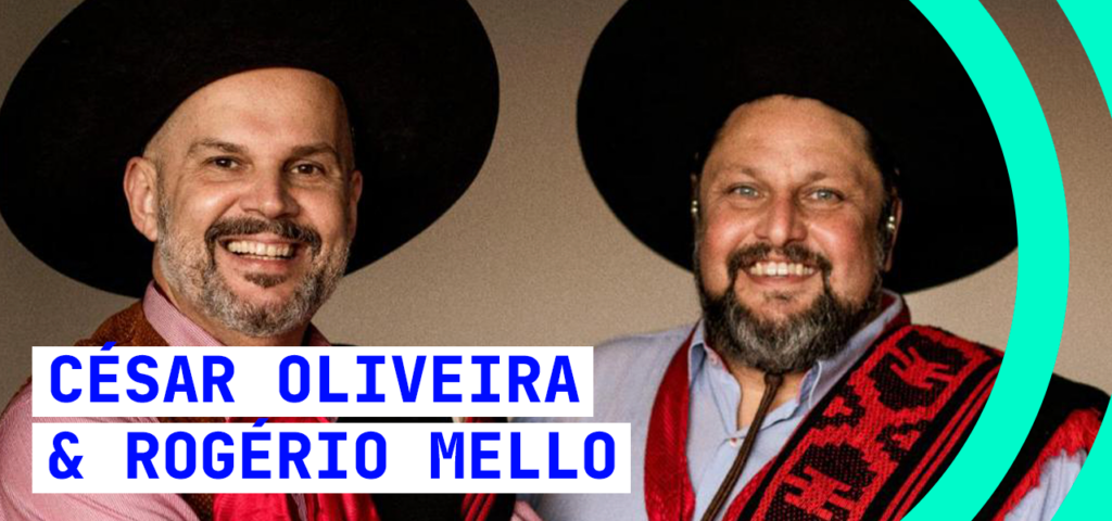
A music concert by César Oliveira & Rogério Mello, a popular Brazilian Gaucho music duo from Rio Grande do Sul state, where the Minuano wind blows, and from where Chip in the Minuano will be streamed.

The plastic artist Mauro Vila Real, gaucho, born in 1975, Academic of History by Faccat, became known for his illustrations and works of art. He has worked for publishers such as Marvel and DC Comics, between 2011 and 2014, on world-renowned titles such as Superman and Wolverine, as well as music album covers, posters, websites, comics, newspapers and books.
The music concert and live painting will be fully virtual on August, 24th at 7:20 pm (UTC-3) at the Minuanoverse.
CLOSING & AWARDS – August 26th
18:00 – 19:00 – Closing & Awards
Location: SBMicro Cadence Auditorium
Closing Ceremony and Awards
Best Papers Awards
IoT Student Contest Award
CTD Awards
Pe. Landell de Moura Award
Chip in 2023 Announcement
Location: SBMicro Cadence Auditorium