Invited 1 – SBMICRO
Wednesday, Aug 28th, 14:20 – 15:00, Room A
 Ravi Todi, Western Digital, USA
Title: Emerging technologies to drive next semiconductors industry revelation
Abstract
The pace of technological change has again reached an inflection point setting the stage for a new era of dramatic innovation in the semiconductor industry. Emerging technologies and growth applications such as 5G, artificial intelligence, machine learning, autonomous vehicles, mobility and IoT will continue to generate massive amounts of data that needs to be captured, preserved, accessed and transformed. The relentless pace of innovation will continue to fuel requirements for robust data infrastructure. Although traditional Moore’s Law scaling remains important, the complexity of this next inflection point requires a new perspective on silicon scaling. Changing market demands are also driving innovation in differentiated technologies and system-level integration approaches that will be combined with silicon technology scaling.
This presentation will examine the economic trends reshaping the industry and explore the technology directions that can successfully produce the needed innovations.
Bio
Ravi Todi received his M.S. degree in electrical and mechanical engineering and his doctoral degree in electrical engineering from university of central Florida (UCF), Orlando – Florida. His graduate research work was focused on gate stack engineering, with emphasis on binary metal alloys as gate electrode and on high mobility germanium channel devices. In his early career as, advisory engineer/scientist at semiconductor research and development center (SRDC) at IBM microelectronics division his work was focused on high performance embedded dynamic random access memory (eDRAM) integration on 45nm silicon on insulator (SOI) logic platform. For his many contributions to the success of eDRAM program at IBM, Ravi was awarded IBM’s prestigious outstanding technical achievement award. In 2012 Ravi Joined Qualcomm for 20nm product development and foundry management, responsible for Qualcomm’s foundry engagement with a leading foundry, owning from test chips, to IP validation, to new product introduction and product yield ramp. In 2015, he joined GLOBALFOUNDRIES, as director of 14nm product line management, where he and his team were responsible for driving the technical and business results of the 14nm FinFET product offerings. Currently he is with Western Digital as Sr. Technologist responsible for foundry technology development for global ASICs.With over 60 US granted patents, over 30 peer reviewed journal publications, over 40 international conference presentations and over 50 invited distinguished lectures, Ravi is well known in semiconductor industry as technical/business leader. He is a distinguish lecturer for IEEE electron devices society and serves as an editor for IEEE transactions on electron devices. He has also served as an IEEE EDS officer-Treasurer for four years, as elected board of governors’ member and currently is vice president for technical activities and conferences.
Invited 2 – SBMICRO
Thursday, Aug 29th, 9:00 – 9:40, Room A
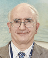 Eddy Simoen, imec (Belgium)
Title: Device-Based Threading Dislocation Assessment in Germanium Hetero-Epitaxy
Abstract
A review on the electrical activity of extended defects and, more specifically, threading dislocations in germanium hetero-epitaxial layers is reported here. Focus is on the impact of some basic types of devices, like a p-n junction diode, a Metal-Oxide-Semiconductor (MOS) capacitor and a Fin-Field-Effect Transistor (FinFET) fabricated in Ge-on-Si. A good understanding of the impact on the leakage current and lifetime in p-n diodes will be shown. Deep-Level Transient Spectroscopy on Ge MOScaps enables the investigation of bulk and interface states related to threading dislocations Finally, the application of Generation-Recombination (GR) noise spectroscopy to the study of GR centers in strained and relaxed Ge-on-Si FinFETs will be illustrated.
Bio
Eddy Simoen received the Master’s and Ph.D. degrees in engineering from the University of Ghent, Ghent, Belgium, in 1980 and 1985, respectively. His dissertation was on the study of trap levels in high-purity germanium by deep-level transient spectroscopy. In 1986, he joined the Interuniversity Microelectronics Center (IMEC), Leuven, Belgium, to work on low-temperature electronics. He is currently an IMEC Scientist, working on defect and strain engineering in high-mobility and epitaxial substrates, and defect studies in germanium. He has coauthored over 1400 journal and conference papers, 9 book chapters, and a monograph on Radiation Effects in Advanced Semiconductor Devices and Materials (Springer, 2002). His current research interests include device physics and defect engineering in general, with particular emphasis on low-frequency noise, low-temperature behavior, and radiation defects in semiconductor components and materials. Dr. Simoen was a Coeditor of two international conference proceedings and a Lecturer at the International Noise School held at IMEC in 1993 and at the ENDEASD Workshop held in Santorini, Greece, (April 1999) and Stockholm, Sweden (June 2000).
Invited 3 – SBMICRO
Thursday, Aug 29th, 11:20 – 12:00, Room A
 Rita Rooyackers, ClaRoo, Leuven, Belgium
Title: Trends and challenges in Tunnel-FETs for low power electronics
Abstract
The quest for low power electronics has driven extensive research on alternative device architectures like Tunnel-FETs. They promise a subthreshold swing (SS) smaller than 60mV/dec and are therefore considered as interesting candidates to replace MOSFETs for low-power applications.
Silicon-based TFETs were most attractive because they allow the re-use of the existing expertise in fabricating high-quality silicon-compatible gate dielectrics as used for MOSFETs. The road ahead was challenging and because of the large discrepancy between the experimental results and the predictions, different TFET architectures were proposed and will be discussed: vertical versus horizontal TFET integration; the short gate TFET and the pocketed line-TFET. However, the small band-to-band-tunneling efficiency in large-bandgap silicon still results in low on-currents. New materials, such as III-V compounds or germanium, featuring lower bandgaps and smaller effective mass, are needed to improve the tunneling efficiency. To enhance the on-currents while maintaining a silicon-channel, the incorporation of heterostructures to decrease the effective tunneling barrier was proposed and will be discussed: e.g. the integration and results of a germanium-source silicon-channel TFET, which acts as an n-TFET maintaining the low off-currents of an all-silicon TFET.
Since most group IV (Si, SiGe, Ge) TFETs do not fulfil the requirements of SS and I ON , materials like In(Ga)As and Ga(As)Sb are studied because of the higher tunneling generation rate due to their direct bandgap. Besides, III-V materials offer a wide array of possibilities for band engineering with hetero-structures for both n-type or p-type TFET operation. They also provide a higher tunneling efficiency.
Integration schemes and results for different III-V TFET architectures will be discussed for different III-V materials and horizontal versus vertical integration. Apart from III-V semiconductors, 2D-materials like e.g. MoS 2 are currently being investigated for possible application in TFETs. Simulations show that their relative low dielectric constant is beneficial to improve the SS as well as the I ON . Present status and main challenges are reviewed.
Bio
Rita Rooyackers received in 1975 the B.S. degree in industrial chemistry from the Rega Institute, Katholieke Universiteit Leuven (KU Leuven), Belgium, and followed the basics of VLSI processing of the postgraduate education program in Microelectronics Engineering at the KU Leuven. From 1976 until 1984, she was with the ESAT laboratory of the KU Leuven. In 1984, she joined the research center imec in Leuven, working in the field of deep sub-micron CMOS technology and exploratory devices in both silicon and III-V semiconductors. She actively participated in several European projects and the imec core partner programs. She holds more than 30 European and American patents and has authored and co-authored more than 300 papers. Since 2018 she is an independent consultant in semiconductor process technology.
Invited 4 – SBMICRO
Thursday, Aug 29th, 14:20 – 15:00, Room A
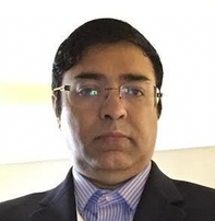 Anirban Bandyopadhyay,
Director, RF Strategic Applications & Business Development, GLOBALFOUNDRIES, Inc., USA
Title: Silicon Technologies for 5G Enhanced Mobile Broadband Radio interface on mmWave
Abstract
5G, the next generation cellular standard will cover different usage scenarios covering enhanced mobile broadband (eMBB), ultra-reliable, low latency communication (uRLLC) and low power massive machine-to-machine communication (mMTC). In this talk, I’ll focus on eMBB aspect of 5G particularly the mmWave based eMBB. The talk will highlight the need for mmWave based mobile communication, different hardware architecture options and key figures of merits for the radio interface of mmWave 5G eMBB. The focus of the talk will be discussing different chip partitioning options and how different silicon technologies like partially and fully depleted SOI, Silicon-Germanium BiCMOS can address the requirements and challenges for different mmWave 5G radio architectures for both User Equipments (UE) and Infrastructure (small cell, backhaul).
Bio
Dr. Anirban Bandyopadhyay is the Director, RF Strategic Applications & Business Development within GLOBALFOUNDRIES, USA and is located at Hopewell Junction, New York. His work is currently focused on hardware architecture & technology evaluations and business development for different RF and mmWave applications. Prior to joining GLOBALFOUNDRIES, he was with IBM Microelectronics for 8 years where he used to manage design enablement group for wireless applications and also led RF strategic applications and marketing. During 2000-2007, Dr. Bandyopadhyay was with Intel, California where he worked on different areas like Silicon Photonics, signal integrity in RF & Mixed signal SOC’s. Dr. Bandyopadhyay did his PhD in Electrical Engineering from Tata Institute of Fundamental Research, India and Post-Doctoral research at Simon Fraser University and Nortel, Canada and at Oregon State University, USA. He has many publications in international journals and conferences, wrote a book chapter on Optical Photodetectors and holds several US patents. He represents Global Foundries in different industry consortia on RF/mmWave applications and is a Distinguished Lecturer of IEEE Electron Devices
Society.
Invited 5 – SBMICRO
Friday, Aug 30th, 11:20 – 12:00, Room A
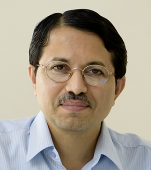 Navakanta Bhat,
Centre for Nano Science and Engineering (CeNSE)
Title: 2D Nano materials for CMOS compatible Gas Sensors
Abstract
Among the 2D materials family, the Transition Metal Dichalcogenides (TMD) offer interesting opportunities for application in chemi-resistive gas sensors. Along with high surface to volume ratio, an ideal characteristic for surface adsorption driven gas sensing phenomenon, TMDs lend themselves for wide range of tunability of other important parameters such as bandgap and conductivity. In order to build CMOS compatible gas sensors for system-on-chip applications, it is also important to develop low temperature processes for the integration of sensing materials at the back end of the CMOS line. In this context liquid exfoliation of 2D TMD materials can be exploited for room temperature synthesis of sensing material on top of CMOS platform. We present high performance gas sensors realized using few layer WS2 and WSe2 for NH3 and H2S gases respectively.
Bio
Navakanta Bhat received his Ph.D. in Electrical Engineering from Stanford University, Stanford, CA in 1996. Then he worked at Motorola’s Networking and Computing Systems Group under Advanced Products R&D Lab (APRDL) in Austin, TX until 1999. At Motorola he worked on logic technology development and he was responsible for developing high performance transistor design and dual gate oxide technology. He joined the Indian Institute of Science, Bangalore in 1999 where he is currently a Professor and Chair, Centre for Nano Science and Engineering. His current research is focused on Nanoelectronics device technology, Biosensors for point of care diagnostics and Gas sensors for pollution monitoring. He has 240 research publications in international journals and conferences and 10 granted US patents and 14 pending patents to his credit. He was instrumental in creating the National Nanofabrication Centre (NNfC) at IISc, Bangalore, benchmarked against the best university facilities in the world. He served as the chairman of NNfC administration committee from 2010 to 2015.
He is an elected Fellow of the Indian National Academy of Engineering and Fellow of IEEE. He is currently a member of the Board of Governors of the IEEE Electron Devices Society and also the Chair of Nanotechnology technical committee. He was the Editor of IEEE Transactions on Electron Devices, (2013-2015), and the chief-editor of the IEEE TED special issue on “2D Materials for Electronic, Optoelectronic and Sensors”. He is a Distinguished Lecturer of the IEEE Electron Devices Society.
His research has been recognized by several awards. Notable among them include Dr. Abdul Kalam Technology Innovation National Fellowship (2018), Prof. Rustum Choksi award for Excellence in Engineering Research (2017), Nina Saxena Technology Excellence award (2018), NASI Reliance Industries Platinum Jubilee award (2018) and BIRAC Innovator award (2018). He has also received the prestigious Infosys Prize (2018) for his contributions in Engineering and Computer Science category. He is the founder and promoter of a startup company, PathShodh Healthcare Pvt Ltd (www.pathshodh.com). Based on his group’s research in biosensors, PathShodh has developed the first of its kind multi-analyte point-of-care diagnostic device for 5 blood tests and 3 urine tests, related to multiple chronic diseases including diabetes and its complications, anemia and malnutrition, kidney and liver diseases. For this technology, PathShodh has received multiple recognitions : Confederation of Indian Industry (CII) Industrial Innovation Award 2017, for the most promising start-up and CII Grand Jury Award for Innovation, 2017; Federation of Indian Chambers of Commerce and Industry (FICCI) Healthcare Excellence award, 2017 for the best start-up of the year; Design Impact award for Social change by Titan.
Invited 1 – SBCCI
Wednesday, Aug 28th, 14:20 – 15:00, Room B
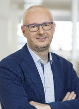 Riccardo Mariani
VP, Industry Safety, NVIDIA Corporation
Title: Trusting Smart Machines
Abstract
Smart Machines and the related cognitive technologies (such as AI) are changing our life by offering new ways to interact with computing systems. However, we expect Smart Machines to deliver services that can justifiably be trusted. This expectation (so called “dependability”) includes attributes such as reliability, availability, functional safety, safety of the intended functionality, security and time determinism. The talk willgive an overview of existing (such as ISO 26262, IEC 61508) and new (such as ISO 21448, ISO/SAE 21434, UL 4600) standardization activities, aimed to provide a framework for building interoperable dependable Smart Machines. The talk will highlight the major challenges of applying those standards and which additional innovations may be required.
Bio
Riccardo Mariani is widely recognized as an expert in functional safety and integrated circuit reliability. In his current role as chief functional safety technologist at Intel Corporation, he oversees strategies and technologies for IoT applications that require functional safety, high reliability and performance, such as autonomous driving, transportation and industrial systems. Riccardo Mariani has been recently nominated 2019 VP of IEEE Computer Society Standardisation Activities.
Mariani spent the bulk of his career as CTO of Yogitech, an industry leader in functional safety technologies. Before co-founding the Italian company in 2000, he was technical director at Aurelia Microelettronica, where his responsibilities included leading high-reliability topics in projects with CERN in Geneva. A prolific author and respected inventor in the functional safety field, Mariani has contributed to multiple industry standards efforts throughout his career, including leading the ISO 26262-11 part specific to semiconductors. He has also won the SGS-Thomson Award and the Enrico Denoth Award for his engineering achievements. He holds a bachelor’s degree in electronic engineering and a Ph.D. in microelectronics from the University of Pisa in Italy.
Invited 2 – SBCCI
Thursday, Aug 29th, 11:20 – 12:00, Room B
 Hussam Amrouch
CES /KIT – Karlsruhe Institute of Technology – Germany
Title: Negative Capacitance Transistor (NCFET) to Rescue Technology Scaling
Abstract
The inability of MOSFET transistors to switch faster than 60mV/decade, due to the nonscalable Boltzmann factor, is one of the key fundamental limits in physics for technology scaling. This is, in fact, the bottleneck in voltage scaling, which has led o the discontinuation of Dennard’s scaling. As a result, on-chip power densities have continuously increased and the operating frequency of processors stopped improving in the last decade to prevent unsustainable on-chip temperatures. In this talk, we will demonstrate how improvements in the electrical characteristics of transistors, obtained in emerging technologies, can be investigated from physics, where they do originate, all the way up to the system level, where they ultimately affect the efficiency of computing.
We will focus on the Negative Capacitance FET (NCFET), which is an emerging technology that pushes the sub-threshold swing to below its fundamental limit, can revive the prior trends in processor design with respect to voltage and frequency scaling. We will focus on answering the following three key questions to draw the impact of NCFET technology on computing efficiency: In how far NCFET technology will enable processors (i) to operate at higher frequencies without increasing voltage?, (ii) to operate at higher frequencies without increasing power density?, and (iii) to operate at lower voltages, while still fulfilling performance requirement? The latter is substantial for IoT devices, where available power budgets are extremely restricted.
Bio
Dr. Hussam Amrouch is a Research Group Leader at the Chair for Embedded Systems (CES), Karlsruhe Institute of Technology (KIT), Germany, where he is leading of the Dependable Hardware research group. He received his Ph.D. degree from KIT in 2015 with highest distinction (Summa cum laude). His main research interests are emerging technology and design for reliability from physics to the system level. He published so far around 55 publications in physics, circuit and CAD communities. He holds seven HiPEAC Paper Awards. He has three best paper nominations at DAC’16, DAC’17 and DATE’17 for his work on reliability. He currently serves as Associate Editor at Integration, the VLSI Journal.
Invited 3 – SBCCI
Friday, Aug 30th, 11:20 – 12:00, Room B
 Bernardo Culau, Director of Characterization
Silvaco, Brazil
Title: On-Chip Variation and the Sign-off Timing Flow: An Industry Perspective
Abstract
As semiconductor technology advances, the impact of on-chip variation increases and, thus, requires more sophisticated solutions. Although these challenges need to be handled while considering a variety of issues, such as feasible run times in production usage, the over-riding consideration is how to reduce pessimism. Each new approach by the industry is intended to reduce over-pessimism from a previous one (whereas run time is a driving factor), but all come with trade-offs. In this talk, we will present the industry perspective of these major challenges, showing the progress up to the current accepted solutions and what is next. Finally, we will also discuss how Silvaco’s R&D team in Brazil has been addressing these leading-edge challenges.
Bio
Bernardo Culau is Director of Characterization at Silvaco. He joined Silvaco in 2018 as part of the acquisition of Nangate where he had worked for 9 years. At Nangate he developed EDA tools for library characterization and delivered standard cell library IP for multiple foundries and technology nodes. Bernardo holds Computer Engineering degrees from Universidade Federal do Rio Grande do Sul, Brazil and from Grenoble INP, France.
Invited 1 – INSCIT
Wednesday, Aug 28th, 16:40 – 17:20, Room C
 Flávio Henrique Vasconcelos
Minas Gerais Federal University, Brazil
Title: Making Measurements Naturally Better: new definitions of the SI base units
Abstract
The SI – the International System of units – for historical reasons, was defined in terms of seven base units and the derived units were products of powers of the base units. The base units, regarded as dimensionally independent are: the metre, the kilogram, the second, the ampere, the kelvin, the mole, and the candela. A decision taken at the 26th meeting of the General Conference of Weights and Measures (CGPM) leading to the greatest change since 1960 when SI was established, came into force after May 20, 2019 and now all the SI units are defined in terms of some well-known natural constants. The seven defining constants of the SI are: Δν Cs ,
the caesium hyperfine frequency; c, the speed of light in vacuum; h, the Planck constant; e, the elementary charge; k, the Boltzmann constant; N A , the Avogadro constant; and K cd , the luminous efficacy of a defined visible radiation. The role for the base units continues in the present even though the SI itself is now defined in terms of the defining constants above.
The complete system of units can be derived from the fixed values of these defining constants, expressed in the units of the SI. These seven defining constants are the most fundamental feature of the definition of the entire system of units and certainly will open up the way for the use of new technologies, including quantum technologies, to implement the definitions. The new definitions come with no prescription of particular realization methods and this allows the development of new and more accurate measurement techniques.
Short bio:
He received the B.Sc. and the M.Sc. in electrical engineering from the Federal University of Minas Gerais, Belo Horizonte, Brazil and the Ph.D. from the University of Manchester, U.K. He is currently a full Professor with the Department of Electrical Engineering at the Federal University of Minas Gerais, Brazil.
His interest lies in electrical metrology, quantum hall effect in graphene for portable electrical resistance standards, wireless sensor networks for application in agriculture and health and data acquisition. He has led many projects in metrology, instrumentation and electric engineering education, in particular the one entitled BITIB – a program sponsored by INMETRO that awarded scholarships to more than 150 students from the Federal University of Minas Gerais in many metrology and instrumentation areas in a period of four years.
Invited 2 – INSCIT
Thursday, Aug 29th, 9:00 – 9:40, Room C
 Khaled Nabil Salama
King Abdullah University of Science and Technology (KAUST)
Title: Biosensors using nanomaterials
Abstract
Biosensor development includes the deposition of (nano)materials onto a conductive electrode surface, which is a crucial step for obtaining improved performance from the constructed biosensors. Various methods have been used to create a successful matrix of (nano)materials that ensures proper contact between the material and electrode surface. The purpose of (nano)material deposition is to provide a high surface area to improve the electroanalytical performance of biosensors by supporting the stable immobilization of enzymes in a more significant quantity as well as enhancing the catalytic or bioaffinity features. In this talk, we summarized the methods used for (nano)material deposition onto an electrode surface for efficient biosensor fabrication. An enhanced and optimized (nano)material deposition method is crucial for the mechanical stability and fabrication reproducibility of electrodes when designing a suitable biosensing device. In addition, we discussed the problems faced during biosensor application as well as the present challenges and prospects for superior deposition methods.
Short bio:
Khaled N. Salama received the B.S. degree from the Department Electronics and Communications, Cairo University, Cairo, Egypt, in 1997, and the M.S. and Ph.D. degrees from the Department of Electrical Engineering, Stanford University, Stanford, CA, USA, in 2000 and 2005, respectively. He was an Assistant Professor at Rensselaer Polytechnic Institute, NY, USA, between 2005 and 2009. He joined King Abdullah University of Science and Technology (KAUST) in January 2009, where he is now an associate professor, and was the founding Program Chair until August 2011. His work on CMOS sensors for molecular detection has been funded by the National Institutes of Health (NIH) and the Defense Advanced Research Projects Agency (DARPA), awarded the Stanford–Berkeley Innovators Challenge Award in biological sciences and was acquired by Lumina Inc. He is the author of 300 papers and 20 patents on low-power mixed-signal circuits for intelligent fully integrated sensors and neuromorphic circuits using memristor devices.

