TUTORIALS (free of charge)
All SBMICRO TUTORIALs is sponsored by IEEE/Electron Device Society
IEEE EDS Minicolloquium
Tutorial 1 – SBMICRO
Tuesday, Aug 27th, 9:00 – 10:40, Room A and B
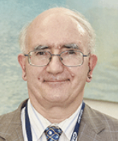 Eddy Simoen, imec (Belgium)
Topic: Low-frequency noise of advanced CMOS devices.
Abstract
Interest in low-frequency noise has increased significantly in recent years, even for CMOS logic devices, as it has become a source of temporal variability. In addition, it is an important parameter for analog and RF circuit applications. In this lecture, the basic sources of LF noise will be described, namely, white noise, generation-recombination (GR) and Random Telegraph Noise (RTN), corresponding with a Lorentzian spectrum and, finally, 1/f or flicker noise. The different models for 1/f noise will be described: either mobility fluctuations or carrier number fluctuations, corresponding with charge exchange between the channel and traps in the gate oxide. In the framework of the McWhorter theory, 1/f noise in a MOSFET is generated by tunneling to and from traps in the gate oxide, at different distances from the interface with the semiconductor. Ways to distinguish between the two mechanisms will be described. In practice, most CMOS devices behave according to the n model, so that the 1/f noise can be considered as a probe for the oxide trap density and for the gate stack quality in general. This also implies that LF noise can be used as an analytical tool to assess the traps in the gate stack. For scaled devices, also time-domain RTN measurements can serve that purpose. Assuming purely elastic tunneling, one can transform a 1/f noise spectrum into an oxide trap density profile versus depth, where typically traps between 1 and 2 nm from the interface contribute to the spectral density. RTN can provide even more information, when studied as a function of temperature or gate and drain bias. This yields the activation energy for carrier capture and emission and can provide information on the exact location of the underlying single trap. The issue of elastic/inelastic tunneling will also be addressed. As will be discussed, RTN in FinFETs can be caused not only by a single gate oxide trap but also by a single trap in the semiconductor fin. Guidelines to distinguish the two types of RTN will be described.
In a second part of the lecture, LF noise and RTN spectroscopy is applied to several types of MOSFETs and how processing affects the noise spectrum and power spectral density. It is shown that the prime factor in determining the noise behavior is the gate stack, whereby high- materials usually correspond with a one to two decades higher 1/f noise. It will be shown that equally important is the choice of the gate metal, with the polysilicon/SiO2 combination corresponding with the low-noise reference condition. In addition, it will be shown that the implementation of so-called threshold voltage shifters, consisting of metal-oxide cap layers can also drastically change the LF noise behavior. Besides the type of materials, also the integration (gate first or last) can have an impact on the noise PSD. Finally, it will be shown that the implementation of some post-deposition treatments, like an SF6 plasma can improve the noise PSD and, hence, reduce the effective oxide trap density. A final important factor is the type of channel material: replacing silicon by so-called high-mobility materials goes hand in hand with increased defectivity. This is a consequence of the lattice mismatch between silicon and foe example germanium. Deposition of Ge on a silicon platform will lead to the introduction of threading and misfit dislocations, which can affect the noise performance, by introducing GR noise.
Bio
Eddy Simoen received the Master’s and Ph.D. degrees in engineering from the University of Ghent, Ghent, Belgium, in 1980 and 1985, respectively. His dissertation was on the study of trap levels in high-purity germanium by deep-level transient spectroscopy. In 1986, he joined the Interuniversity Microelectronics Center (IMEC), Leuven, Belgium, to work on low-temperature electronics. He is currently an IMEC Scientist, working on defect and strain engineering in high-mobility and epitaxial substrates, and defect studies in germanium. He has coauthored over 1400 journal and conference papers, 9 book chapters, and a monograph on Radiation Effects in Advanced Semiconductor Devices and Materials (Springer, 2002). His current research interests include device physics and defect engineering in general, with particular emphasis on low-frequency noise, low-temperature behavior, and radiation defects in semiconductor components and materials. Dr. Simoen was a Coeditor of two international conference proceedings and a Lecturer at the International Noise School held at IMEC in 1993 and at the ENDEASD Workshop held in Santorini, Greece, (April 1999) and Stockholm, Sweden (June 2000).
Tutorial 2 – SBMICRO
Tuesday, Aug 27th, 11:20 – 13:00, Room A and B
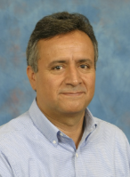 Fernando Guarín, GlobalFoundries, USA
Topic: Leveraging semiconductor technology for the benefit of society
Abstract
Thanks to relentless scaling, coupled along with advances in materials and process integration of semiconductor devices have enabled the exponential growth of applications enabling sensors and information technologies that have transformed society. The level of instrumentation grows daily with ever increasing intelligence and ability to communicate and automate many processes and industries in what is now known as the Internet of Things (IoT). Thanks to these advances the world is smaller and flatter. The reality of living in a globally integrated world is upon us and is presenting us with many opportunities and challenges. This increased information content gives us a unique path to alleviate and find solutions to the problems of many of the most important issues facing the world today. These advances must remind us that we are all now connected – economically, technically and socially. But we are also learning that just being connected may not be sufficient. We must solve many problems. As engineers, we have the knowledge and the responsibility to do so. In this talk, we will discuss how Semiconductor technology and electron devices have benefited society and the world in which we live. The multiple advances in devices and materials have provided us with unprecedented amounts solutions and information at continually decreasing costs. We will provide tangible evidence that illustrates how electron devices are influencing society, enabling us to better use the energy in a more sustainable manner and changing our interaction with other people near and far. We are now able to provide many people the ability to have access to advanced technology even in the most remote corners of the planet. We must leverage these advances to expand educational opportunities while helping to preserve a sustainable and greener environment. We will provide information on initiatives and access to funding for engineering projects at the local level. Ultimately we must always bear in mind that the large number of scientific and technological advances must produce tangible results for the benefit and progress of humanity.
Bio
Dr. Fernando Guarín is a Distinguished Member of Technical Staff at Global Foundries in East Fishkill New York. He retired from IBM’s SRDC after 27 years as Senior Member of Technical Staff. He earned his BSEE from the “Pontificia Universidad Javeriana”, in Bogotá, Colombia, the M.S.E.E. degree from the University of Arizona, and the Ph.D. in Electrical Engineering from Columbia University, NY He has been actively working in microelectronic reliability for over 35 years.
From 1980 until 1988 he worked in the Military and Aerospace Operations division of National Semiconductor Corporation. In 1988 he joined IBM’s microelectronics division where he worked in the reliability physics and modeling of Advanced Bipolar, CMOS and Silicon Germanium BiCMOS technologies. He is currently leading the team qualifying GlobalFoundries RF 5G technology offerings.
Dr. Guarín is an IEEE Fellow, Distinguished Lecturer for the IEEE Electron Device Society EDS, where he has served in many capacities including; member of the IEEE’s EDS Board of governors, chair of the EDS Education Committee, Secretary for EDS. He is the EDS President 2018-2019.
Tutorial 3 – SBMICRO
Tuesday, Aug 27th, 14:20 – 16:00, Room A and B
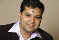 Ravi Todi, Western Digital, USA
Sr. Technologist for Foundry Technology Development
Topic: Semiconductor Industry: A story of unprecedented growth, and we are just getting started!
Abstract
Many have argued that the golden era of semiconductor technology scaling has ended, however in this presentation I will attempt to present the counter arguments. For the semiconductor industry, connectivity (5G), the Internet of Things (IoT) and high bandwidth data processing now promise to be the enablers for the next phase of growth. However, the industry has reached a new level of maturity that demands new innovations in computing, connectivity, system integration and ultra-low power applications. Although traditional Moore's Law scaling remains important, the complexity of this next inflection point requires a new perspective on silicon scaling. Changing market demands are also driving innovation in differentiated technologies and system-level integration approaches that will be combined with silicon technology scaling. This presentation will examine the economic trends reshaping the industry and explore the technology directions that can successfully produce the needed innovations. We will draw lessons from five decades of semiconductor industry, dive deep into technical challenges facing future technology scaling, and attempt to formulate a roadmap for next decade of silicon technology.
Bio
Ravi Todi received his M.S. degree in electrical and mechanical engineering and his doctoral degree in electrical engineering from university of central Florida (UCF), Orlando – Florida. His graduate research work was focused on gate stack engineering, with emphasis on binary metal alloys as gate electrode and on high mobility germanium channel devices. In his early career as, advisory engineer/scientist at semiconductor research and development center (SRDC) at IBM microelectronics division his work was focused on high performance embedded dynamic random access memory (eDRAM) integration on 45nm silicon on insulator (SOI) logic platform. For his many contributions to the success of eDRAM program at IBM, Ravi was awarded IBM’s prestigious outstanding technical achievement award. In 2012 Ravi Joined Qualcomm for 20nm product development and foundry management, responsible
for Qualcomm’s foundry engagement with a leading foundry, owning from test chips, to IP validation, to new product introduction and product yield ramp. In 2015, he joined GLOBALFOUNDRIES, as director of 14nm product line management, where he and his team were responsible for driving the technical and business results of the 14nm FinFET product offerings. Currently he is with Western Digital as Sr. Technologist responsible for foundry technology development for global ASICs. With over 60 US granted patents, over 30 peer reviewed journal publications, over 40 international conference presentations and over 50 invited distinguished lectures, Ravi is well known in semiconductor industry as technical/business leader. He is a distinguish lecturer for IEEE electron devices society and serves as an editor for IEEE transactions on electron devices. He has also served as an IEEE EDS officer-Treasurer for four years, as elected board of governors’ member and currently is vice president for technical activities and conferences.
Tutorial 4 – SBMICRO
Tuesday, Aug 27th, 16:40 – 18:20, Room A and B
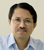 Navakanta Bhat, Indian Institute of Science
Topic: Electrochemical Biosensors for Point-of-Care Diagnostics
Abstract
In this tutorial, I will first give an overview of biosensors technology for point-of-care diagnostics applications. Various transduction methods such as electrochemical, optical, acoustic, mechanical, calorimetric and ISFET based techniques will be reviewed in the context of bioanalytes ranging from DNA, proteins, pathogens and other markers. The importance of receptor selection in designing the biosensor will be highlighted. Subsequently I will describe, in depth, our fascinating journey in the last few years, on the development of nonenzymatic and non antibody based electrochemical biosensors traversing through scientific discovery, engineering innovation, entrepreneurial venture and manufacturing scale-up to create one of its kind multi-analyte point of care diagnostic device “lab-on-palm”. This lab on palm is capable of addressing multiple chronic diseases including diabetes, kidney and liver disease, anemia and malnutrition. This device is capable of performing 5 blood tests (Hb, HbA1c, Serum Albumin, Glycated Albumin, Glucose) and 3 urine tests (Microalbuminuria, Urine Creatinine and Urine ACR (www.pathshodh.com). The low cost electrochemical sensing technology, which uses disposable test strips can potentially bridge healthcare divide with a capability to perform blood and urine tests anywhere, anytime, in remote and resource challenged areas.
Bio
Navakanta Bhat received his Ph.D. in Electrical Engineering from Stanford University, Stanford, CA in 1996. Then he worked at Motorola’s Networking and Computing Systems Group under Advanced Products R&D Lab (APRDL) in Austin, TX until 1999. At Motorola he worked on logic technology development and he was responsible for developing high performance transistor design and dual gate oxide technology. He joined the Indian Institute of Science, Bangalore in 1999 where he is currently a Professor and Chair, Centre for Nano Science and Engineering. His current research is focused on Nanoelectronics device technology, Biosensors for point of care diagnostics and Gas sensors for pollution monitoring. He has 240 research publications in international journals and conferences and 10 granted US patents and 14 pending patents to his credit. He was instrumental in creating the National Nanofabrication Centre (NNfC) at IISc, Bangalore, benchmarked against the best university facilities in the world. He served as the chairman of NNfC administration committee from 2010 to 2015.
He is an elected Fellow of the Indian National Academy of Engineering and Fellow of IEEE. He is currently a member of the Board of Governors of the IEEE Electron Devices Society and also the Chair of Nanotechnology technical committee. He was the Editor of IEEE Transactions on Electron Devices, (2013-2015), and the chief-editor of the IEEE TED special issue on “2D Materials for Electronic, Optoelectronic and Sensors”. He is a Distinguished Lecturer of the IEEE Electron Devices Society.
His research has been recognized by several awards. Notable among them include Dr. Abdul Kalam Technology Innovation National Fellowship (2018), Prof. Rustum Choksi award for Excellence in Engineering Research (2017), Nina Saxena Technology Excellence award (2018), NASI Reliance Industries Platinum Jubilee award (2018) and BIRAC Innovator award (2018). He has also received the prestigious Infosys Prize (2018) for his contributions in Engineering and Computer Science category. He is the founder and promoter of a startup company, PathShodh Healthcare Pvt Ltd (www.pathshodh.com). Based on his group’s research in biosensors, PathShodh has developed the first of its kind multi-analyte point-of-care diagnostic device for 5 blood tests and 3 urine tests, related to multiple chronic diseases including diabetes and its complications, anemia and malnutrition, kidney and liver diseases. For this technology, PathShodh has received multiple recognitions : Confederation of Indian Industry (CII) Industrial Innovation Award 2017, for the most promising start-up and CII Grand Jury Award for Innovation, 2017; Federation of Indian Chambers of Commerce and Industry (FICCI) Healthcare Excellence award, 2017 for the best start-up of the year; Design Impact award for Social change by Titan.
Tutorial 1 – SBCCI/INSCIT
Tuesday, Aug 27th, 9:00 – 10:40, Auditorium
 Edmar Candeia Gurjão
Federal University of Campina Grande
Topic: Compressed Sensing: theory, implementation and challenges
Abstract
Compressed Sensing is a technique to acquire signals proposed in the last decade that is becoming a mature field, with some important applications like Radar and Magnetic Resonance Imaging and others. In spite of advances in its theoretical foundations, hardware implementation and applications Compressed Sensing area still has open questions and unexplored utilizations. Based on the expertise developed at Federal University of Campina Grande (UFCG) in the Compressed Sensing development and applications, in this tutorial it will be presented the background theory of Compressed Sensing with emphasis in the essential concepts, hardware implementations of the Analog to Information Converters, with emphasis on the UFCG developed hardware, and also open questions in the theory and applications of Compressed Sensing as the development of Analog to Information Converters.
Bio
Graduated in Electrical Engineering from Federal University of Paraíba (1996), master’s in Electric Engineering from Federal University of Paraíba (1999) and PhD in Electrical Engineering from Federal University of Campina Grande (2003). In 2012 was visiting professor at Department of Electrical Engineering, Notre Dame University (USA). Actually is associate professor of the Department of Electrical Engineering at Federal University of Campina Grande and collaborator at the Professional Master Degree Course in Science and Technology at Paraíba State University. Expertise in Compressed Sensing, Software Defined Radio, Applied Signal Processing and Applications of Linear Algebra. Senior Member of IEEE and member of the Brazilian Society of Telecommunications (SBRT). Co-author of the book Introduction to Signal and Systems (In Portuguese), Elsevier, 2015 and Digital Signal Processing, Momentum Press, 2019.
Tutorial 2 – SBCCI
Tuesday, Aug 27th, 11:20 – 13:00, Auditorium
 Hussam Amrouch
CES /KIT – Karlsruhe Institute of Technology – Germany
Topic: Design for Reliability in the Nano-CMOS Era
Abstract
Due to aging, circuit reliability has become extraordinary challenging. Reliability-aware circuit design flows do virtually not exist and even research is in its infancy. In this presentation, first we will demonstrate how we can bring aging awareness to existing EDA tool flows based on so-called degradation-aware cell libraries. These libraries include detailed delay information of gates/cells under the impact that aging has on the key parameters of MOSFET transistors. We will also demonstrate that degradation-aware libraries and tool flows are indispensable for not only accurately estimating guardbands, but also efficiently containing them. Then, we will explain how to our degradation-aware cell libraries can be employed within the standard tool flows to quantify the impact of aging at the system level in the context of image processing. This goes far beyond investigating aging with respect to circuits’ path delays solely as often done in state of the art. Afterwards, we will demonstrate how nondeterministic aging-induced timing errors can be converted into deterministic and controlled approximations instead. This enables designers for the first time to narrow or even remove guardbands through exploring application of approximate computing principles in the context of aging. Finally, we will demonstrate how the existing view of aging in the state of the art needs to updated. In fact, aging has been, traditionally, assumed to be a long-term reliability degradation in which its effects are observed in the order of months and years. However, in the deep nano technology, aging has shifted from a sole long-term to a short- and long-term reliability challenge. We will explain why circuits designers need to take that into account when employing guardbands (i.e. safety margins) at the design time. Otherwise, reliability cannot be sustained at runtime.
Bio
Hussam Amrouch is a Research Group Leader at the Chair for Embedded Systems (CES), Karlsruhe Institute of Technology (KIT), Germany, where he is leading of the Dependable Hardware research group. He received his Ph.D. degree from KIT in 2015 with highest distinction (Summa cum laude). His main research interests are emerging technology and design for reliability from physics to the system level. He published so far around 55 publications in physics, circuit and CAD communities. He holds seven HiPEAC Paper Awards. He has three best paper nominations at DAC’16, DAC’17 and DATE’17 for his work on reliability. He currently serves as Associate Editor at Integration, the VLSI Journal.
Tutorial 3 – SBCCI
Tuesday, Aug 27th, 14:20 – 16:00, Auditorium
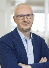 Riccardo Mariani
VP, Industry Safety, NVIDIA Corporation
Topic: On Dependability of Smart Machines
Abstract
A smart machine is a device embedded with machine-to-machine (M2M), human-to-machine (H2M) and cognitive computing technologies such as artificial intelligence (AI), machine learning (ML) or deep learning (DL), all of which it uses to reason, problem-solve, make decisions and even, ultimately, take action. Smart machines include robots, self-driving cars and other cognitive computing systems that are designed to work through tasks with very limited or even without human intervention. The tutorial will provide an overview on smart machines and will focus on their dependability, including reliability, functional safety and cybersecurity, from SW to transistor level.
Bio
Riccardo Mariani is widely recognized as an expert in functional safety and integrated circuit reliability. In his current role as chief functional safety technologist at Intel Corporation, he oversees strategies and technologies for IoT applications that require functional safety, high reliability and performance, such as autonomous driving, transportation and industrial systems. Riccardo Mariani has been recently nominated 2019 VP of IEEE Computer Society Standardisation Activities.
Mariani spent the bulk of his career as CTO of Yogitech, an industry leader in functional safety technologies. Before co-founding the Italian company in 2000, he was technical director at Aurelia Microelettronica, where his responsibilities included leading high-reliability topics in projects with CERN in Geneva. A prolific author and respected inventor in the functional safety field, Mariani has contributed to multiple industry standards efforts throughout his career, including leading the ISO 26262-11 part specific to semiconductors. He has also won the SGS-Thomson Award and the Enrico Denoth Award for his engineering achievements. He holds a bachelor’s degree in electronic engineering and a Ph.D. in microelectronics from the University of Pisa in Italy.
Tutorial 4 – SBCCI
This tutorial 4 is sponsored by CEDA/IEEE
Tuesday, Aug 27th, 16:40 – 18:20, Auditorium
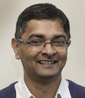 Sachin Sapatnekar
Univ. of Minnesota
Topic: Reliability, Error-resilience, and Approximation in Integrated Systems
Abstract
As CMOS technology matures, the problem of building fully reliable circuits has become more challenging, as a variety of mechanisms that perturb system performance have come into play. These range from ”one-time” drifts due to process variations, which shift circuit performance, to ”run-time” shifts caused by aging mechanisms, which cause degradations and/or failures in devices and interconnects. Developing design mechanisms that model and overcome these shifts requires an understanding from the device level, circuit level, system level, and application level.
At the device level, methods that comprehend performance shifts due to statistical as well as deterministic variations due to process and aging are key. At the circuit level, these must be factored into statistical and intelligent corner-based performance analysis approaches, as well as mechanisms that enable post-silicon compensation. At the system level, compensation and redundancy schemes must be utilized to ensure that the system operates at the desired performance, within a specified power budget.
An equally important consideration arises from application-level requirements. While some mission-critical applications, or segments of applications, require absolute accuracy, many emerging applications (e.g., signal filtering, image/video operations, neuromorphic applications) show a good deal of error-resilience, implying that absolute accuracy is not essential. In these scenarios, it is possible to selectively ignore ”accidental” errors due to process and aging, or even introduce deliberate errors in hardware to build approximate systems that provide just enough accuracy for the application. Using a case study approach, it will be shown how application-level considerations will be used to approximate systems that optimize power and performance within a specified error budget.
Bio
Sachin Sapatnekar is an IEEE Fellow, full professor at Univ. of Minnesota, and a CEDA Distinguished Lecturer. He received the B. Tech. degree from the Indian Inst. of Technology, Bombay, in 1987, the M.Sc. from Syracuse University in 1989, and the Ph. D. degree from the University of Illinois at Urbana-Champaign in 1992. He worked at Texas Instruments during the summer of 1990, and at Intel Corporation during the summer of 1997. He was an Assistant Professor in the Department of Electrical and Computer Engineering at Iowa State University from 1992 to 1997. He is currently a Professor in the Department of Electrical and Computer Engineering at the University of Minnesota, where he holds the Robert and Marjorie Henle chair and the Distinguished McKnight University Professorship. His current research interests lie in developing efficient techniques for computer-aided design of integrated circuits and are primarily centered around physical design, timing and simulation issues, and optimization algorithms. He has served on the editorial boards of several IEEE journals, including as Editor-in-Chief of the IEEE Transactions on CAD. He was a Technical Program Co-chair in 2006 and 2007 for the Design Automation Conference (DAC), and the General Chair in 2010. He has also been the Technical Program Chair and General Chair for the International Symposium on Physical Design (ISPD) and the Tau workshop, and Program Chair for the International Conference on VLSI Design in India. He is a recipient of the NSF Career Award, the SRC Technical Excellence Award, the SIA University Researcher Award, Best Paper Awards at the DAC’97, ICCD’98, DAC’01 DAC’03, ISPD’09, ISQED’10, and ASYNC’16 conferences, a Best Poster Award at IRPS’12, and the ICCAD Ten-Year Retrospective Most Influential Paper Award in 2013 and 2016. He has been a Fulbright Senior Researcher at Universitat Politècnica de Catalunya in Barcelona in 2013, and a DJ Gandhi Visiting Professor at the Indian Institute of Technology, Bombay in 2014. He is a Fellow of the IEEE (2003) and the ACM (2016).

