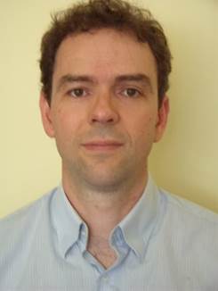
Gilson Inacio Wirth
Federal University of Rio Grande do Sul – Brazil
Wednesday, Aug. 29 – 13:40h – Malbec A

Gilson Wirth
SBCCI INVITED TALK:
Charge Trapping Phenomena in MOSFETS: From Noise to Bias Temperature Instability
Charge capture and emission by defects (traps) close to the Dielectric-Semiconductor interface is known to be the major source of low-frequency noise in modern MOS devices. It is also known to play a role in Bias Temperature Instability (BTI). The basics mechanisms involved in charge trapping and de-trapping will be presented, including a critical discussion of key parameters such as trapping/de-trapping time constants and the amplitude of the fluctuations induced by single traps. Standard low-frequency noise models used today (e.g. BSIM) do not properly model noise behavior under large signal excitation, and often do not to properly model noise variability. A novel physics based modeling and simulation approach will be presented. It is based on the relevant microscopic quantities that play a role in both low-frequency noise and BTI. The modeling approach is valid at both DC and large signal (AC) biasing, and may be applied to time domain (transient) and frequency domain (AC) analysis. Mutual relation between the different reliability phenomena (low-frequency noise, BTI and random dopant fluctuations – RDF) is also studied. For instance, RDF may exacerbate the impact of BTI and low-frequency noise on circuit performance. Additionally, the LF-noise (and BTI) levels from device-to-device can vary several orders of magnitude in deeply-scaled devices, making variability a major concern in advanced MOS technologies. Therefore, to assure proper circuit design in this scenario, it is necessary to identify the fundamental mechanisms responsible for variability in LF-noise and BTI. We introduced a new variability-based analysis, employing the autocorrelation of multiple LF-Noise spectra in terms of parameters such as frequency, bias and temperature. This technique reveals information about the mechanisms responsible for the LF-noise (and BTI) that is difficult to obtain otherwise.
Speaker’s Biography:
Gilson I. Wirth received the B.S.E.E and M.Sc. degrees from the Universidade Federal do Rio Grande do Sul, Brazil, in 1990 and 1994, respectively. In 1999 he received the Dr.-Ing. degree in Electrical Engineering from the University of Dortmund, Dortmund, Germany.
He is currently a professor at the Electrical Engineering Department at the Universidade Federal do Rio Grande do Sul – UFRGS (since January 2007), where he was the head of graduate and undergraduate courses.
From July 2002 to December 2006 he was professor and head of the Computer Engineering Department, Universidade Estadual do Rio Grande do Sul (UERGS).
He is currently a Distinguished Lecturer of the IEEE Electron Devices Society. He was a Distinguished Lecturer of the IEEE Circuits and Systems Society (term 2010 to 2011).
His research work is focused on reliability and yield of MOS devices and circuits, including low-frequency noise, bias temperature instability (BTI), radiation effects, and design techniques to improve yield and reliability.
He has stablished successful collaborative work with different companies and research groups in Europe, North and South America.
