Program
Plenary Speakers
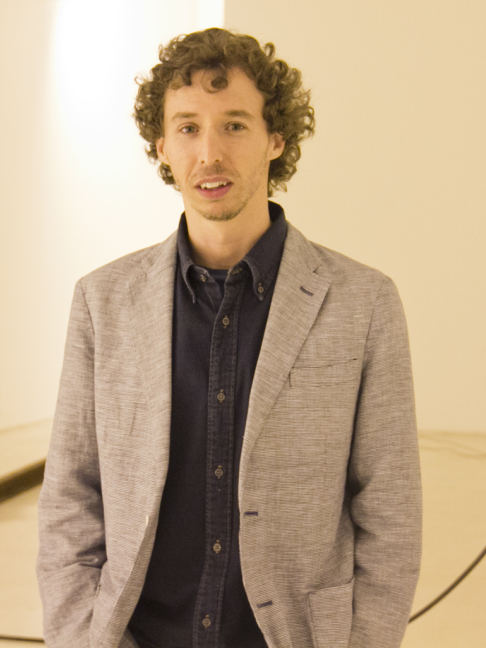
Otavio Schipper
Recent projects at the intersections of art, science and technology
Otavio Schipper holds a degree in Physics from Universidade Federal do Rio de Janeiro. He has received the KLAS Award from the Max Planck Society in 2017 and the Berlin Fellowship from the Akademie der Künste in 2015. Schipper has been invited as a Guest Artist by the Arts at CERN (European Organization for Nuclear Research) program in 2019.
The talk will present recent projects at the intersections of art, science and technology such as “Mechanical Unconscious”, a sound installation consisting of a real-time dialogue between old-fashioned telegraph machines, synthetic voices and telephone sounds, sometimes blurring, sometimes imposing the limits between natural and artificial language.
Through the presentation of ready-made objects such as antique telegraph machines, tuning forks, eyeglasses, elevator cabins and electric poles, Otavio Schipper’s work connects past physical worlds with our present mental landscapes. The realms of imagination become present in installations that deal with the perception of time and the cultural memory of objects, leading to the questioning of boundaries between fiction and reality. In Schipper’s installations, the spectator often experiences a spectrum of sensations, from enlightenment to nostalgia. Elements of hard science and technologies from different periods lead the viewer into territories more closely associated with dream states and imagination dives, instead of a systematic organization of knowledge in the form of testable explanations and predictions about the universe.
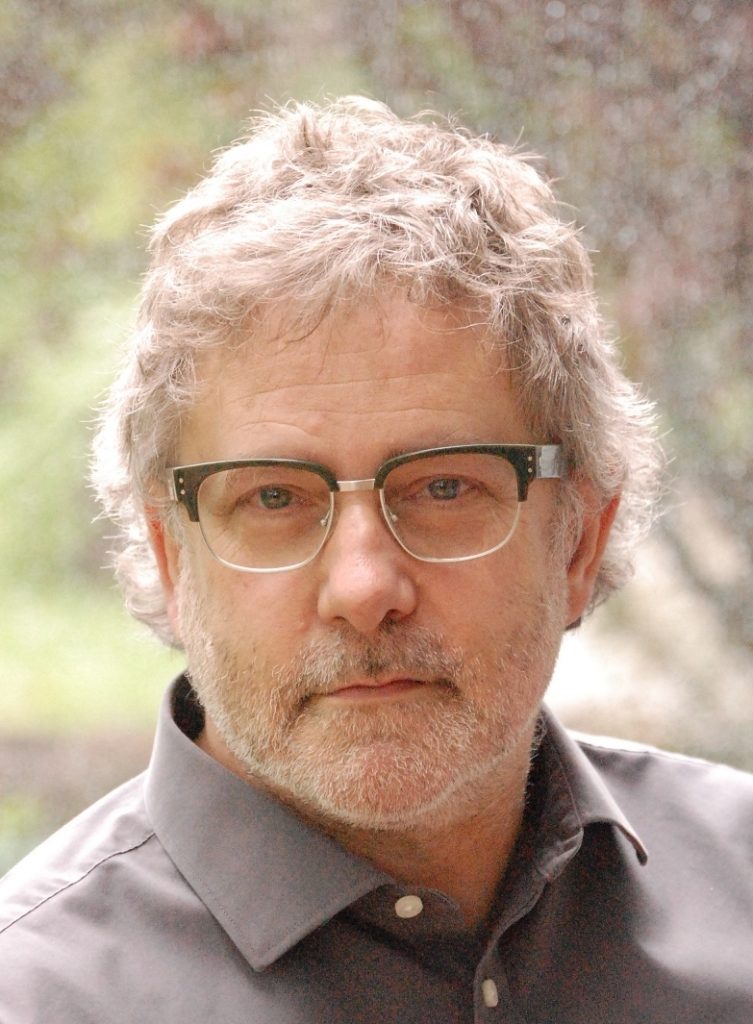
Gottfried Strasser,
TU-Wien, Austria
On-Chip Sensing with Monolithically Integrated Quantum Cascade Devices
This talk aims to give a short introduction in the field of quantum devices with a strong focus on quantum cascade lasers (QCLs) and quantum cascade detectors (QCDs). Since the first proposal using intraband transitions in QWs to achieve lasing intraband and interband cascade lasers have been intensively studied in terms of bandstructure engineering, cavity design and fabrication technology. Nowadays, QC lasers are compact and coherent light sources covering the spectral range from the mid-infrared to the terahertz region.
Today, photonic devices are widely used in environmental and industrial process control and/or monitoring as well as medical and biochemical diagnostics. Conventional optical sensing setups include a light source, a light-analyte interaction region and a separate detector. We developed and improved a sensor concept based on a bi-functional quantum cascade heterostructure, for which the differentiation between laser and detector is eliminated. Apart from the fascinating physics of light-matter interaction, this enables mutual commutation of laser and detector, simplifies remote sensing setups and allows crucial miniaturisation of sensing devices for further integration.

Peter Beerel,
University of Southern California, USA
Efficient and Trustworthy AI at the Edge
The super-linear increase of deep learning model size with the slow-down of Moore’s law has made their deployment at the edge on resource-constrained devices exceedingly challenging. In particular, to ensure the increasing demand for trustworthiness in various personalized and safety-critical applications, AI at the edge must not only be energy-efficient but also robust and privacy-preserving. In this talk, I will first discuss recent advances of our group in model compression strategies yielding efficient yet robust models. In particular, our foundational work on dynamic network rewiring demonstrated generation of DNN models with SoTA robustness against gradient-based perturbations with up to an order of magnitude reduced compute and storage costs. I will then discuss model linearization strategies that target latency-efficient privacy-preserving machine learning as a service (PPMLaS). As operating ReLUs in PPMLaS costs > 100x more computational and latency compared to regular inference, our linearization strategies identify and trim unimportant ReLUs, yielding PPMLaS-friendly neural networks that require up to ~10x fewer ReLUs without significant accuracy drop. We then leverage our novel ReLU sensitivity to first propose a joint depth and ReLU reduction method of DNNs to further reduce the latency and compute. Finally, I will summarize advances from our group in the area of brain-inspired spiking neural networks in both static and dynamic vision tasks. In particular, I will discuss the novel training frameworks that our group developed for both conversions from pre-trained ANNs as well as training SNNs from scratch. Coupled with novel sparsity-friendly accumulator-based hardware architectures, SNNs have the potential to provide trustworthy solutions with significantly reduced inference energy and latency and negligible accuracy drop for a wide range of applications compared to non-spiking networks.
Short Bio
Dr. Peter A. Beerel received his B.S.E. degree in EE from Princeton University, Princeton in 1989 and his M.S. and Ph.D. degrees in EE from Stanford in 1991 and 1994, respectively. Dr. Beerel is currently a Full Professor and Associate Chair of the Computer Engineering Division of the Ming Hsieh ECE Department at the University of Southern California. He is also a Research Director at USC’s Information Sciences Institute. He co-founded TimeLess Design Automation to commercialize an asynchronous ASIC flow in 2008 and sold the company in 2010 to Fulcrum Microsystems which was bought by Intel in 2011. His interests include Hardware Security, Machine Learning, and the intersection of the two. He has published over 170 papers, recently spanning top HW venues (TCAD, DAC, HOST, CHES) and top ML conferences (ICLR, WACV, ICCV, NeurIPS). His students have won several best paper awards and he is a Senior Member of the IEEE.
Valeriya Kilchytska,
Université Catholique de Louvain, Belgium
Advanced SOI-based MOSFETs for Analog and RF applications: electrical characterization perspectives
Enormous progress of the semiconductor technology we observe over the last decades was mostly driven by the continuous demand for the increase of the operation speed and integration density of complex digital circuits. Aggressive device downscaling has requested the introduction of new channel and gate stack materials as well as non-classical device architectures. Two main contenders have emerged to satisfy IRDS requirements for device nodes towards 20 nm and beyond: planar fully depleted (FD) Silicon-on-Insulator (SOI) with ultra-thin body (UTB) and ultra-thin buried oxide (BOX), so called UTBB MOSFETs and multiple-gate (MuG) MOSFET (FinFETs and nanowire (NW) FETs). While digital aspects of these new architectures are widely addressed, their perspectives for analog and RF applications stay often in a shadow.
This talk does not target to compare different advanced MOSFETs, but rather review methodological approaches enabling a fair assessment of novel device architectures for their analog and RF performance. Those approaches are shown to be different from the traditionally used ones for the assessment of the device perspectives for digital applications. Based on the original research realized by our group over the last years, advantages and necessity of those techniques will be demonstrated on different study cases of various advanced MOSFETs in a wide temperature range from cryogenic, 4 K up to 250°C. A wide frequency band characterization (from DC up to hundred GHz range) will be positioned as a key element enabling a fair device assessment towards analog and RF applications. Importance of the thermal effects in deeply scaled devices, its fair assessment and possible ways of reduction will be discussed. Harmful effect on the performance of advanced MOSFETs arising from the “extrinsic” parasitic elements and thus the need for a proper separate extraction of “intrinsic” vs. “extrinsic” device parameters will be pointed out.
Short Bio
Dr. Valeriya Kilchytska is Senior Researcher at Université catholique de Louvain (UCLouvain), Louvain-la-Neuve, Belgium. She assures presently a research logistic lead of WELCOME Characterization Technological Platform of UCLouvain.
She received her MSc in solid-state electronics and Ph.D. degree in semiconductor and dielectric physics from Kiev Shevchenko University, Ukraine, in 1992 and 1997, respectively. Her Ph.D. work, performed at the Institute of Semiconductor Physics (ISP), Kyiv, was devoted to the investigation of electrical and radiation properties of SOI structures. From 1997 to 2001, she worked on the investigation of bias-temperature and injection processes in the buried oxides. In 1996 and 2000 she was a visiting researcher at UCL, for high-temperature and generation-recombination processes in SOI devices. In 2001, she was a visiting postdoctoral researcher at the Chalmers University of Technology, Sweden, for characterization of SiC MOS structures. In 2002, she joined UCL for characterization and simulation of advance SOI devices.
She has a long-term experience in advanced device characterization focused on wide frequency band characterization, simulation and performance assessment from one side and on the investigation of wide-temperature range behavior and radiation effects particularities of advanced devices from another side. She has been a principal investigator of numerous research projects funded by regional and European institutions. She has authored or co-authored more than 250 technical papers and conference contributions. She also serves as a reviewer for various international journals and conferences such as IEEE TED, IEEE EDL, Solid State Electronics, … and a TPC member of several international conferences. She is an elected Deputy Director of SINANO Institute (www.sinano.eu), nonprofit Association established in 2008 as a durable EU Network of researchers in order to form a distributed Centre of Excellence in the nanoelectronic field.
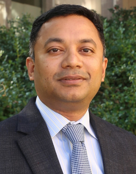
Mohammad Abdullah Al Faruque,
University of California Irvine, USA
Cross-Layer Security of Embedded and Cyber-Physical Systems
Cyber-physical systems (CPS), such as automotive, manufacturing, and power grid systems, are engineered systems built from and depend upon the seamless integration of computation and physical components. Embedded systems comprising hardware and software systems are the primary enabling technology for these cyber-physical systems. Moreover, when cyber-physical systems get connected to the Internet, it forms the Internet-of-Things (IoT). Today, CPSs can be found in security-sensitive areas such as aerospace, automotive, energy, healthcare, manufacturing, transportation, entertainment, and consumer appliances. Compared to the traditional information processing systems, due to the tight interactions between cyber and physical components in CPSs and closed-loop control from sensing to actuation, new vulnerabilities emerge from the boundaries between various layers and domains. In this seminar, Dr. Al Faruque will discuss how new vulnerabilities emerge at the intersection of multiple components and subsystems and their different hardware, software, and physical layers. Several recent examples from various cyber-physical systems (e.g., an automotive system) will be presented in this talk. To understand these new vulnerabilities, a very different set of methodologies and tools are needed. Defenses against these vulnerabilities also demand new hardware/software co-design approaches. The seminar will highlight recent developments in this regard. This seminar’s primary goal will be to highlight various research challenges and the need for novel scientific solutions from the EDA research community and definitely from the larger embedded systems, cyber-physical systems, distributed computing systems, and computer architecture research communities.
Short Bio
Mohammad Al Faruque received his B.Sc. degree in Computer Science and Engineering (CSE) from Bangladesh University of Engineering and Technology (BUET) in 2002, and M.Sc. and Ph.D. degrees in Computer Science from Aachen Technical University and Karlsruhe Institute of Technology, Germany in 2004 and 2009, respectively. He is currently with the University of California Irvine (UCI) as an Associate Professor and Directs the Embedded and Cyber-Physical Systems Lab. He served as an Emulex Career Development Chair from October 2012 till July 2015. Before, he was with Siemens Corporate Research and Technology in Princeton, NJ as a Research Scientist. His current research is focused on the system-level design of embedded and Cyber-Physical-Systems (CPS) with a special interest in low-power design, CPS security, data-driven CPS design, etc. He is the author of 2 published books. Besides many other awards, he is the recipient of the School of Engineering Mid-Career Faculty Award for Research 2019, the IEEE Technical Committee on Cyber-Physical Systems Early-Career Award 2018, the IEEE CEDA Ernest S. Kuh Early Career Award 2016, Thomas Alva Edison Patent Award 2016 from the Edison Foundation, the 2016 DATE Best Paper Award, the 2015 DAC Best Paper Award, and the 2009 IEEE/ACM William J. McCalla ICCAD Best Paper Award. He is also the recipient of the UCI Academic Senate Distinguished Early-Career Faculty Award for Research 2017 and the School of Engineering Early-Career Faculty Award for Research 2017. Besides 120+ IEEE/ACM publications in the premier journals and conferences, he holds 9 US patents. Moreover, his work has been featured in the New York Times, the Los Angeles Times, Newsweek, ACM Communication, Science Magazine, etc., among many other national and international newspapers and magazines. Prof. Al Faruque’s research is currently funded by NSF, NIH, DOE, DoD, DARPA, DOT, DoEd, ONR, UCOP, Caltrans, and several industries. Among many important professional service roles, Dr. Al Faruque is the program chair of the premier conference ACM/IEEE International Conference on Cyber-Physical Systems (ICCPS) 2021, the general chair for ICCPS 2022, program vice-chair for ACM/IEEE International Conference on Hardware/Software Codesign and System Synthesis (CODES+ISSS) 2022, and the program chair for CODES+ISSS 2023.
IEEE CASS Rio de Janeiro Workshop: Current Trends in IC Design

Prof. Fernando Silveira,
Universidad de la República, Uruguay
Ratio based analog/RF design: a generalization of gm/ID and Inversion Coefficient methods
Design methods for analog integrated circuits based on gm/ID have the key feature of being based on a magnitude (the gm/ID ratio) that provides information about the transistor operation independently of its width (W, letting aside very narrow transistors rarely applied in analog design) and length (L), except for a slight dependence on L in short channel devices. A general characteristic for the transistors of a given length in a given process is obtained. Therefore, it gives a global view and orientation about the design space. This makes it very suitable for helping the designer to gain insight on how to tune the design and, particularly, aiding novel designers to quickly find their way in the analog design art. The same applies to the, somehow “dual”, inversion coefficient (IC) based methods. Both methods are based on magnitudes (gm/ID and IC) that are ratios (or proportional to ratios) of key magnitudes of the transistor operation.
Extensions and evolutions of the gm/ID method have, implicitly or explicitly, identified this “ratio based characteristic” and have shown the advantages of considering other key ratios of magnitudes that share the same characteristics as gm/ID of being W independent. The approach presented is particularly appropriate for nanoscale devices where multiple unitary devices in parallel are usually applied.
This talk will provide an overview on these ratio based analog design approaches, contributing to show a general vision about them. These methods originally targeted small signal analog design. In the talk it will be shown examples of extension of the basic idea to nonlinear RF blocks (power amplifiers and envelope detectors) as well as to distortion analysis.
Short Bio
Fernando Silveira received the electrical engineering degree from Universidad de la República, Montevideo, Uruguay, in 1990, and the M.Sc. and Ph.D. degrees in microelectronics from Université catholique de Louvain, Louvain-la-Neuve, Belgium, in 1995 and 2002, respectively. He is currently a Professor with the Electrical Engineering Department, Universidad de la República. His research interests include the design of ultra-low-power analog and RF integrated circuits and systems, in particular with biomedical application. In this field, he has co-authored two books and many technical papers. He has had multiple industrial activities including leading the design of an application specified integrated circuit for implantable pacemakers and designing analog circuit modules for implantable devices for various companies worldwide, field in which he continues to do consulting. He was member of the Technical Advisory Board of Gtronix, Inc, USA from 2006 to 2010, received the “Ingeniero Destacado” (Distinguished Engineer) award by the Uruguayan Association of Engineers in 2007 and was a member for 2011-2012 of the Distinguished Lecturers Program of the IEEE Circuits and Systems Society. Since 2017 he is a member of the Honorary Committee of the National Researchers System of Uruguay.

Prof. Ricardo Reis,
Universidade Federal do Rio Grande do Sul, Brazil
Physical Design: New Solutions Inspired in the Past
By the end of years ‘70s, microprocessors were designed by hand, showing na excellent layout compaction. It will be presented some highlights of the reverse engineering of the Z8000, which control part was designed by hand, showing several layout optimization strategies as well an optimization of the number of transistors. The observation of the Z8000 layout inspired the research of methods to do the automatic generation of the layout of any transistor network, allowing to reduce the number of transistors to implement a circuit, and by consequence, the leakage power consumption. Power Optimization is a keyword in the IoT world. Some of the layout automation tools developed by our group are briefly presented. It will also be presented why the use of visualization tools can help to improve the quality of EDA tools and to improve the quality of the solution.
Short Bio
Ricardo Reis received a Bachelor degree in Electrical Engineering from Federal University of Rio Grande do Sul (UFRGS), Porto Alegre, Brazil, in 1978, and a Ph.D. degree in Microelectronics from the National Polytechnic Institute of Grenoble (INPG), France, in 1983. Doctor Honoris Causa by the University of Montpellier in 2016. He is a full professor at the Informatics Institute of Federal University of Rio Grande do Sul. His main research includes physical design automation, design methodologies, fault tolerant systems and microelectronics education. He has more than 700 publications including books, journals and conference proceedings. He was vice-president of IFIP (International Federation for Information Processing) and he was also president of the Brazilian Computer Society (two terms) and vice-president of the Brazilian Microelectronics Society. He is an active member of CASS and he received the 2015 IEEE CASS Meritorious Service Award. He was vice-president of CASS for two terms (2008/2011). He is the founder of the Rio Grande do Sul CAS Chapter, which got the World CASS Chapter of The Year Award 2011, 2012, 2018 and 2022, and R9 Chapter of The Year 2013, 2014, 2016, 2017 and 2020. He is a founder of several conferences like SBCCI and LASCAS, the CASS Flagship Conference in Region 9. He was the General or Program Chair of several conferences like IEEE ISVLSI, SBCCI, IFIP VLSI-SoC, ICECS, PATMOS. Ricardo was the Chair of the IFIP/IEEE VLSI-SoC Steering Committee, vice-chair of the IFIP WG10.5 and he is Chair of IFIP TC10. He also started with the EMicro, an annually microelectronics school in South Brazil. In 2002 he received the Researcher of the Year Award in the state of Rio Grande do Sul. He is a founding member of the SBC (Brazilian Computer Society) and also founding member of SBMicro (Brazilian Microelectronics Society). He was member of CASS DLP Program (2014/2015), and he has done more than 70 invited talks in conferences. Member of IEEE CASS BoG and IEEE CEDA BoG. He is the CASS representative at the IEEE IoT TC. Ricardo received the IFIP Fellow Award in 2021 and the ACM/ISPD Lifetime Achievement Award in 2022. He received the 2023 IEEE CASS John Choma Educational Award.
Victor Grimblatt,
R&D Group Director and General Manager, Synopsys, Chile
The Tangled Tree of Technology
Charles Darwin’s “tree of life” is a model used to represent the “vertical evolution”: in Darwin’s “tree of life”, each new generation inherits the parental genes, the strongest, most favorable genes sprout, while the weakest become extinct. There is a “tree of technology” too. In truth, there are many; among the most notable are CMOS, and xPU. In these “trees of technology”, each new generation inherits the parental “genes”, unchanged, unchallenged, just smaller (CMOS) or bigger (xPU), an artificial Galapagos Islands ecosystem.
Darwin’s “tree of life” has been challenged by UIUC Prof. Carl Woese, an “evolutionary biologist”, who proposed a more “tangled tree of life”, in which gene transfer, and therefore evolution happens both vertically (VGT), slowly, generation after generation of one organism, and horizontally (HGT), rapidly, across [even radically] different organisms. Over the last four billion years, there have been several bursts of horizontal evolution, among which the “Cambrian explosion”, when practically all major phyla started appearing in the fossil record.
In this talk, I propose that we are at the dawn of a technological “Cambrian explosion”; that we must challenge the established “trees of technology”; that only the entanglement of many [even radically] different “trees of technology” will allow us to leapfrog the fundamental, physical limits that CMOS and xPU, are hitting against.
Short Bio
Victor Grimblatt has an engineering diploma in microelectronics from Institut Nationale Polytechnique de Grenoble (INPG – France) and an electronic engineering diploma from Universidad Tecnica Federico Santa Maria (Chile). He got his PhD on Electronics in 2021 from University of Bordeaux. He is currently R&D Group Director and General Manager of Synopsys Chile. He has published several papers in IoT, EDA, Smart Agriculture, Climate Change, and embedded systems development. Since 2012 he is chair of the IEEE Chilean joint chapter of CASS/EDS/SSCS. He has been part of several conferences TCP (ISCAS, ICECS, LASCAS) and Steering Committees. He is TPC chair of ISCAS 2024. He is member of the IEEE CASS Board of Governors for the period 2021 – 2023. He founded the Electronics for Agrifood SIG at CASS and chairs it. He was Chair of LASCAS Steering Committee from 2018 to 2022. He is CASS representative at the IEEE Climate Change TAB. He was President of the Chilean Electronic and Electrical Industry Association (AIE) from 2017 to 2021. From 2006 to 2008 he was member of the “Chilean Offshoring Committee” organized by the Minister of Economy of Chile. In 2010 he was awarded as “Innovator of the Year in Services Export”. In 2022 he was awarded as “IEEE/AIE Best Engineer” in Chile. In 2023 he was awarded as IEEE R9 Outstanding Engineer”. Victor’s research areas are EDA (Electronic Design Automation), Climate Change, and Smart Agriculture.
SBMicro: Tutorials and Invited Talks
Frank Schwierz,
Technische Universität Ilmenau, Germany
Tutorial: 2D Materials and their Role in Future Electronics
During the past 20 years, 2D (two-dimensional) materials have attracted enormous attention from the scientific community. The rise of these materials began in early 2000s with the work on graphene done at Manchester University. Particularly the observed high carrier mobilities raised early expectations that graphene could be a perfect electronic material and possibly replace the traditional semiconductors in transistor electronics. It soon became clear, however, that due its zero bandgap graphene is not suitable for most electronic devices, in particular transistors. However, researchers soon extended their work to 2D materials beyond graphene, many of them showing sizable bandgaps and therefore beinguseful for transistors. Indeed, the progress of research on 2D transistors was rapid and MOSFETs with semiconducting 2D channels were demonstrated by many groups. Moreover, other types of 2D devices such memristors, sensors, and optoelectronic devices are currently under investigation.
In the present lecture, we first take a look on the early days of graphene research and discuss both accomplishments and misconceptions of this period. Next, an overview of the 2D materials is provided and the potential of 2D transistors is assessed as realistically as possible. To this end, two key material properties – bandgap and mobility – are examined and the mobility-bandgap tradeoff is discussed. The state of the art of 2D transistors is reviewed by summarizing the results of leading groups in the field and by comparing the performance of 2D transistors to that of competing conventional transistors. Outstanding achievements, such as the demonstration of a 1-nm gate MoS2 MOSFET in 2016 (note that this is the transistor with the shortest gate reported ever) and of MOSFETs with stacked 2D nanosheet channels during the very recent past are highlighted. Based on these considerations, a balanced view of both the pros and cons of 2D transistors is provided and their potential in future electronics is discussed. Moreover, the status of beyond-CMOS 2D devices is examined with the example of 2D memristors.
Invited Talk: MOSFETs with Stacked 2D Nanosheet Channels – An Auspicious Option to Delay Forever
At ISSCC 2003, Gordon Moore, at that time Chairman Emeritus of Intel’s Board of Directors, presented a far-sighted seminal paper entitled No Exponential is Forever: But “Forever” Can Be Delayed! Moore stated that the desirable exponential trends related to MOSFET scaling, e.g., the exponential decrease of transistor footprint and the related increase of circuit complexity, cannot be maintained forever. He also said, however, that by smart engineering solutions the lifetime of these trends can be extended and that the key to continuing the historical exponential trends in semiconductor electronics would be developing novel transistor designs and elaborating radically changed MOSFET architectures beyond the planar structures generally used at that time. This is exactly what happened 10 years later when Intel, soon followed by other leading chipmakers, introduced a new MOSFET architecture called FinFET. Meanwhile, however, also FinFET scaling is approaching its limits and the next radical change of the MOSFET architecture is on the agenda.
In the present paper, we provide a brief overview of MOSFET scaling trends, elaborate the motivation for introducing the FinFET in the early 2010s, and examine FinFET scaling. Then we discuss the upcoming transition to another new MOSFET architecture in the 2020s and introduce the stacked nanosheet channel MOSFET, thereby putting special emphasis to transistors using two-dimensional (2D) materials such as 2D TMDCs (transition metal dichalcogenides) for the stacked channels. We discuss the merits, prospects, and challenges of MOSFETs with stacked 2D TMDC channels, summarize the current state of the art of these transistors, and finally provide an outlook on the future of MOSFET scaling.
Short Bio
Frank Schwierz received the Dr.-Ing. and Dr. habil. degrees in 1986 and 2003, respectively. Presently he serves as Privatdozent at Technische Universität Ilmenau, Germany, and his research is focused on novel device and material concepts for future electronics. Dr. Schwierz has been conducting research projects funded by the European Community, German government agencies, private foundations, and the industry. Together with partners from academia and industry, he was involved in the development of the fastest Si-based transistors worldwide in the late 1990s, of Europe’s smallest MOSFETs in the early 2000s, as well as of the fastest GaN HEMTs on Si and the fastest GaN tri-gate HEMTs worldwide in the 2010s. Moreover, his work on two-dimensional materials since 2010 made a major contribution to the current understanding of the merits and drawbacks of these materials for application in electronic devices, in particular transistors.
Dr. Schwierz has published more than 300 journal and conference papers including > 50 invited/keynote papers. He is author of the books Modern Microwave Transistors – Theory, Design, and Performance (J. Wiley & Sons 2003) and Nanometer CMOS (Pan Stanford Publishing 2010) and editor of the book Two-Dimensional Electronics – Prospects and Challenges (MDPI 2016).
Dr. Schwierz is a Senior Member of the IEEE. He served as committee member of international conferences (most notably IEDM 2018 and 2019), as a Distinguished Lecturer of the IEEE Electron Devices Society, and as an editor of the IEEE Transactions on Electron Devices for more than six years. Moreover, he was one of the key contributors to the Emerging Research Devices Technology Working Groups of the 2013 and 2015 ITRS editions.

Dr. Edmundo Gutierrez,
National Institute for Astrophysics, Optics and Electronics, Mexico
Tutorial: From micro-semiconductor devices to the discovery of the black hole in the Milky way
In this talk, the use of micrometric semiconductor devices for the discovery of the huge Milky Way will be introduced. Technical and scientific information on the INAOE’s Large Millimeter Telescope is introduced as well as the use of radiation detectors utilized to detect milli-meter and sub-millimeter radiation coming from outer space.
I describe the design, fabrication, and operation of the 50-meter Large Millimeter Telescope, and how the use of micrometer-sized semiconductor devices is used to observe at 12 million light years.
Invited Talk: Cryogenic characterization and modeling of advanced CMOS technologies at 4.2 K and below
Short Bio
Dr. Edmundo A. Gutiérrez-D. Got his PhD in 1993 from the Catholic University of Leuven, Belgium with the thesis entitled “Electrical performance of submicron CMOS technologies from 300 K to 4.2 K”. From 1989 to 1993, while working for his PhD, served as a research assistant at the Interuniversity Microelectronics Center (IMEC) in Leuven, Belgium. In 1996 was guest Professor at Simon Fraser University, Vancouver, Canada. In 1996 spent two months as an invited lecturer at the Sao Paulo University, Brazil. In 2000 acted as Design Manager of the Motorola Mexico Center for Semiconductor Technology. In 2002 was invited lecturer at the Technical University of Vienna, Austria. In 2005 joined the Intel Mexico Research Center as technical Director. Currently he holds a Professor position at the National Institute for Astrophysics, Optics and Electronics (INAOE), in Puebla, Mexico. Prof. Gutiérrez-D. is an IEEE senior member since 2008.
Professor Gutiérrez-D. has published over 100 scientific publications and conferences in the field of semiconductor device physics, has supervised 5 M.Sc. and 10 Ph.D. thesis, and is author of the book “Low Temperature Electronics, Physics, Devices, Circuits and Applications” published by Academic Press in 2000. Prof. Gutiérrez-D. is member of the Mexico National System of Researchers and technical reviewer for the Mexico National Council for Science and Technology (CONACyT).

Prof. Adam W. Skorek,
University of Québec, Canada
Tutorial: High Performance Quantum Computing in Nanoelectronics
The computation demand in modeling and simulation of electron devices is still growing and it is particularly high in nanoelectronics where nanoscale electro-thermal analysis can be used as an example. Hopefully, the High Performance Computing (HPC) and High Performance Quantum Computing (HPQC) infrastructures become more easily accessible and offer researchers some new opportunities based on the open and shared resources including not only computing facilities with quantum units but also knowledge with currently observed openings in the field of intellectual property issues. Artificial intelligence (AI) is present in electrical, electronics, and computer engineering for years, with current facilities like ChatGPT arrival, which easily define HPQC as development and utilization of quantum computers that can perform complex computations at a significantly faster rate than classical computers. Quantum computing leverages the principles of quantum mechanics, which allow for the representation and manipulation of information using quantum bits, or qubits, instead of classical bits. According to ChatGPT generated answers, the HPQC application in nanoelectronics has the potential to revolutionize various fields and enable new applications with a significant impact in quantum simulation where quantum computers can simulate and model complex systems that are challenging for classical computers. In nanoelectronics, HPQC can be used to simulate the behavior of nanoscale electronic devices and materials accurately. This can aid in the design and optimization of nanoelectronic components, such as transistors, sensors, and memory devices, leading to improved performance and efficiency. As those answers need human instructions, an overview of the current trends and initiatives from a worldwide perspective will be illustrated by the lecturer’s explorations of the HPQC opportunities in nanoelectronics. Some practical examples and instructions for potential users will be presented, inspiring the audience to explore some largely available modern tools.
Short Bio
Prof. Adam Waldemar Skorek, M’87, SM’90, F’09, LF’22, completed Bachelor and Master of Electrical Engineering Program at Białystok University of Technology (Poland) receiving both Master and Engineer degrees in 1980. Participant of the Electrical Engineering Faculty Doctoral Studies, he received a Doctor of Technical Sciences degree in Electrical Engineering at Warsaw University of Technology (Poland) in 1983. From 1983 to 1987 he was a Visiting Lecturer at the Institute of Telecommunications in Oran (Algeria). In 1987, he joined the University of Quebec at Trois-Rivières (UQTR), where currently, he is a Full Professor and Director of the Electro-Thermal Management Laboratory He founded the UQTR’s Electro-Thermal Management Laboratory which succeeded both the NanoHeat Laboratory and the UQTR’s Industrial ElectroHeat Laboratory founded and directed by himself since 1989. He is conducting electrical engineering courses for bachelor, master and Ph.D. students. His research works was granted by NSERC, CFI, FRQNT, MITACS and Industry. He was made contributions to the numerical analysis of electro-thermal phenomena exploring and applying various techniques to electrical apparatus and electronic devices. He published and co-published over 150 papers including works on High Performance Computing applications in electro-thermal analysis. A number of those publications are available at IEEE Xplore. He was a Chair of Canadian Heads and Chairs of Electrical and Computer Engineering Departments. Volunteering for more than 35 years in IEEE, he currently serves as the IEEE Fellow Committee Member and the IEEE Richard Harold Kaufmann Award Chair. The IEEE Fellow, as well Fellow of the Engineering Institute of Canada – he is the recipient of the IEEE RAB/MGA Leadership Award and the IEEE Canada W.S. Read Outstanding Services Award. He is the IEEE Electron Devices Society Distinguished Lecturer. He is the recipient of the IEEE Industry Applications Society Distinguished Service Award (2021). Recipient of the Queen Elizabeth II Diamond Jubilee Medal (Canada, 2012), he received from the Presidents of the Republic of Poland the Gold Cross of Merit (Canada, 2004) and Knight’s Cross of the Order of Merit of the Republic of Poland (Canada, 2015). In 2023, he received from Poland in Chicago, (IL, USA), the Rooster Brotherhood Knightly Order of St. John Cantius.
Andreas Kerber,
Intel, USA
Tutorial: Reliability of Metal Gate / High-K CMOS devices
Aggressively scaled transistor technologies with metal gate/high-k stacks encounter additional reliability challenges beside bias temperature instability (BTI) in PMOS and NMOS devices, time dependent dielectric breakdown and hot carrier degradation. Time-zero variability and variability induced by device aging is a growing concern which needs to be modeled using stochastic processes. The physical nature of the stochastic process remains under debate and to support model development efforts large statistical data sets are essential. In addition, self-heating during reliability testing can be observed in novel device structures like bulk FinFET, SOI FinFETs, FDSOI and gate-all-around devices and needs proper attention. Furthermore, to increase the confidence in the discrete device reliability models, device-to-circuit correlations need to be established. In this presentation we discuss how to obtain stochastic BTI data for discrete SRAM and logic device beyond 3σ, address device-to-circuit correlations using ring-oscillators and explore self-heating effects in FinFET and SOI devices.
Invited Talk: Ring Oscillator Aging Characterization in Conventional CMOS Technologies
Ring Oscillator (RO) aging characterization has become a critical demonstrator for aggressively scaled transistor technologies utilizing metal gate/high-k stacks and FinFETs, FDSOI and gate-all-around device architectures. The introduction of time-resolved RO characterization and enhanced RO designs enabling diagnostic device characterization methods are also found to be beneficial for digital aging characterization in conventional CMOS technologies based on poly-Si/SiON gate stacks. Operating RO circuits at moderate stress conditions confirms aging is dominated by the NBTI mechanism while at elevated stress conditions hot carrier contribution in NMOS devices are observed in thin and thick oxide devices. We will also discuss the post stress recovery effects in RO circuits for both dynamic and static stress modes. Finally, we will correlate device degradation in RO circuits to discrete device degradation utilizing AC stress modes.
Short Bio
Andreas Kerber received his Diploma in physics from the University of Innsbruck, Austria, in 2001, and a PhD in electrical engineering from the TU-Darmstadt, Germany, with honors in 2004. From 1999 to 2000 he was an intern at Bell Laboratories, Lucent Technologies (Murray Hill, NJ, USA) working on the electrical characterization of ultra-thin gate oxides. From 2001 to 2003, he was the Infineon Technologies assignee to International SEMATECH at IMEC in Leuven, Belgium, where he was involved in the electrical characterization of alternative gate dielectrics for sub-100 nm CMOS technologies. From 2004 to 2006, he was with the Reliability Methodology Department at Infineon Technologies in Munich, Germany, responsible for the dielectric reliability qualification of process technology transfers of 110 and 90 nm memory products. During that time, he developed a low-cost, fast wafer-level data acquisition setup for time-dependent dielectric breakdown (TDDB) testing with sub-ms time resolution. From 2006 to 2018 he was working for AMD in Yorktown Heights, NY, and GLOBALFOUNDRIES in Malta and East-Fishkill, NY, as a Principal Member of Technical Staff on front-end-of-line (FEOL) reliability research with focus on metal gate / high-k CMOS process technology, advanced transistor architecture and device-to-circuit reliability correlation. From 2018 to 2019 he was with Skorpios Technologies in Albuquerque, NM, working on reliability of Si-photonic devices. From Nov. 2019 to March 2021, he was with ON-Semiconductor in Santa Clara, CA working on product quality management of CMOS image sensors for automotive, consumer and industrial markets. Since March 2021 he is with Intel in Santa Clara, CA working on CMOS and interconnect reliability for 3D-NAND technology.
Dr. Kerber has contributed to more than 110 journal and conference publications and presented his work at international conferences, including the IEDM, VLSI and IRPS. In addition, he has presented tutorials on metal gate / high-k reliability characterization at the IIRW, IRPS and ICMTS. Dr. Kerber has served as a technical program committee member for the SISC, IRPS, IIRW, IEDM, Infos, ESSDERC, is a Senior Member of the IEEE and a Distinguished Lecturer (DL) for the IEEE Electron Devices Society.
SBCCI: Tutorials

Prof. Ricardo Reis,
Universidade Federal do Rio Grande do Sul, Brazil
Electronic Physical Design Automation – Fundamentals and Challenges
The development of any integrated circuit depends heavily on the quality of the EDA tools used in the design flow. Improved CAD tools and algorithms are needed to cope with new fabrication technology requirements, advanced performance constraints, or simply the enormous number of elements involved. In this tutorial, we will start by giving an overview of the importance of au tomation in the design process. Then some trends on EDA that are needed to deal with the evolution of manufacturing processes will be presented. Basic and advanced optimization strategies for selected physical design problems will be presented. An important aspect of the design is to reduce power consumption at all levels of abstraction. Power optimization is fundamental in nanoCMOS and in the IoT world. At logic and physical levels, one approach that can be used to optimize the circuit, specially reducing static leakage power and using the automatic generation of the cell layout. With on-the-fly cell generation, the same function can be implemented with a reduced number of transistors, requiring less area and significantly optimizing power and performance. A set of tools and algorithms for cell generation will be briefly discussed. Finally, the use of estimation and visualization tools is equally important. They can be applied either in the design flow or just in the tool’s development and research environments as a way to observe and understand the behavior and interactions of algorithms and their operation on real designs and benchmarks.
Target audience:
Graduate and Undergraduate Students, as well professionals from Industry and Academia.
How the intended target audience would benefit from the tutorial:
The audience will have an updated overview of EDA tools for Physical Design, as well an overview about trends to copy with new challenges to cope with new and modern Technologies.
Short Bio
Ricardo Reis received a Bachelor degree in Electrical Engineering from Federal University of Rio Grande do Sul (UFRGS), Porto Alegre, Brazil, in 1978, and a Ph.D. degree in Microelectronics from the National Polytechnic Institute of Grenoble (INPG), France, in 1983. Doctor Honoris Causa by the University of Montpellier in 2016. He is a full professor at the Informatics Institute of Federal University of Rio Grande do Sul. His main research includes physical design automation, design methodologies, fault tolerant systems and microelectronics education. He has more than 700 publications including books, journals and conference proceedings. He was vice-president of IFIP (International Federation for Information Processing) and he was also president of the Brazilian Computer Society (two terms) and vice-president of the Brazilian Microelectronics Society. He is an active member of CASS and he received the 2015 IEEE CASS Meritorious Service Award. He was vice-president of CASS for two terms (2008/2011). He is the founder of the Rio Grande do Sul CAS Chapter, which got the World CASS Chapter of The Year Award 2011, 2012, 2018 and 2022, and R9 Chapter of The Year 2013, 2014, 2016, 2017 and 2020. He is a founder of several conferences like SBCCI and LASCAS, the CASS Flagship Conference in Region 9. He was the General or Program Chair of several conferences like IEEE ISVLSI, SBCCI, IFIP VLSI-SoC, ICECS, PATMOS. Ricardo was the Chair of the IFIP/IEEE VLSI-SoC Steering Committee, vice-chair of the IFIP WG10.5 and he is Chair of IFIP TC10. He also started with the EMicro, an annually microelectronics school in South Brazil. In 2002 he received the Researcher of the Year Award in the state of Rio Grande do Sul. He is a founding member of the SBC (Brazilian Computer Society) and also founding member of SBMicro (Brazilian Microelectronics Society). He was member of CASS DLP Program (2014/2015), and he has done more than 70 invited talks in conferences. Member of IEEE CASS BoG and IEEE CEDA BoG. He is the CASS representative at the IEEE IoT TC. Ricardo received the IFIP Fellow Award in 2021 and the ACM/ISPD Lifetime Achievement Award in 2022. He received the 2023 IEEE CASS John Choma Educational Award.

Sergio Bampi,
Universidade Federal do Rio Grande do Sul, Brazil
Approximate Computing: Advanced VLSI Design Techniques for Energy-Efficient CMOS Accelerators
Approximate computing (AxC) is a digital design technique to improve the performance and energy-efficiency requirements for many applications which inherently tolerate compute errors. Logic design for arithmetic operator approximations and timing-speculative (TS) hardware design techniques are addressed in this talk. TS hardware design paradigm allows either increasing operating frequency or decreasing the voltage beyond the limits determined by static timing analysis (STA), thereby narrowing pessimistic safety margins that conventional Digital VLSI Design methods usually adopt to prevent hardware timing errors. Timing errors need to be evaluated by accurate gate-level simulations, but a significant gap remains in practice: How do these timing errors propagate from the underlying accelerator hardware all the way up to the entire algorithm behavior, where they just may degrade the performance and quality of service of the application at stake?
This Tutorial addresses state-of-the-art developments by the Tutorial Presenter’s group, which innovated in the design of CMOS accelerators for Machine Learning, DNN, and video and image processing.
The tutorial has the following structure:
- Review of Approximate Adders and Approximate Multipliers;
- A cross-layer framework capable of performing investigations of AxC (i.e., from approximate arithmetic, approximate synthesis, or gate-level pruning) linking the algorithms to the VLSI logic design;
- Timing-Speculative digital VLSI hardware design (i.e., voltage over-scaling, frequency over-clocking, temperature margins, and device aging);
- Three design cases and application to illustrate AxC in practice: accelerator for image block matching, accelerator for image filtering, and AI inference engine with decision trees.
The Approximate Computing design framework that will be presented supports the simulation of both timing and logic errors at the gate-level and the behavioral simulation of the algorithms being accelerated dynamically. In the tutorial we present a linking strategy from the VLSI hardware design with the algorithm-level behavior, and vice versa during the evolution of the application runtime. Existing frameworks perform investigations of AxC and TS techniques at circuit-level (i.e., at the output of the accelerator) agnostic to the ultimate impact at the application level (i.e., where the impact is truly manifested), leading to less optimization in the VLSI design. Unlike previous works, the approaches exposed by the presenter offer a holistic assessment of the tradeoff of AxC and TS techniques at the application-level. This framework maximizes energy efficiency and performance by identifying the maximum approximation levels at the application level to fulfill the required good enough quality.
The tutorial, in the last part, illustrates the framework for a few design cases. We present an 8-way SAD (Sum of Absolute Differences) hardware accelerator operating in the HEVC encoder. VOS (Voltage Over-Scaling) applied to the SAD calculations.
The Tutorial exposes and stimulates the audience to explore system-level and circuit-level design approaches for energy-efficiency, so dearly important in CMOS systems-on-chip for IoT devices.
Target audience:
Junior and senior undergraduate students with a basic knowledge of digital logic circuits, Graduate students in Microelectronics.
How the intended target audience would benefit from the tutorial:
The intended target audience will acquire an overview of current and state-of-the art techniques used in accelerators for VLSI digital design of circuits like: dedicated VLSI for deep neural networks, dedicated VLSI circuits for filters of images and videos.
Short Bio
Sergio Bampi received the B.Sc in Electronics Engineering and the B.Sc. in Physics from the Federal Univ. of Rio Grande do Sul (UFRGS, 1979), and the M.Sc. (1982) and Ph.D. degrees in EE from Stanford University (USA) in 1986. Full professor in the Digital Systems and Microelectronics design fields at the Informatics Institute, member of the faculty since 1986. He served as Graduate Program Coordinator (2003-2007), head of research group and projects, technical director of the Microelectronics Center CEITEC (2005-2008) and is the past President of the FAPERGS Research Funding Foundation and of the SBMICRO Microelectronics Society (2002-2006). He is a former member of HP Inc. technical staff, and a visiting research faculty at Stanford University (1998-99) in the USA. His research interests are in the area of ultra-low power CMOS IC design, dedicated complex algorithms, architectures, and ASICs for image and video processing, RF CMOS design and mixed signal IC design for IoT. He has co-authored more than 480 papers in these fields and in MOS devices and EDA. He is a senior member of IEEE, SBC, and SBMICRO societies. He was Technical Program Chair of IEEE SBCCI Symposium (1997, 2005), SBMICRO (1989, 1995), IEEE LASCAS (2013), VARI 2016 Workshops and Conferences.

Jose Silva-Martinez,
Texas A&M University, College Station, USA
Design of Supply Regulators for High Efficiency RF Transmitters
The increasing performance demanded by the emerging wireless communication standards motivates the development of a variety of techniques devoted to improving the efficiency of the power amplifiers since this one of the most power demanding blocks in RF transceivers. Power Amplifier (PA) efficiency improves by modulating its power supply; PA power efficiency is function of the ratio of the voltage amplitude delivered by the PA and the voltage used to bias the amplifier’s output. The envelope tracking modulator maximizes this ratio, correlating the PA output with its power supply. However, efficient modulators must satisfy some critical conditions: i) it must be very agile to track the amplitude variations of PA’s output voltage; ii) The timing mismatch between the PA modulator’s supply and PA output waveform envelope must be reduced to optimize power efficiency and avoid PA saturation and iii) the envelope tracking modulator must be highly power efficient.
In this tutorial,
- Several recently reported envelope tracking techniques are revised;
- The hybrid modulators consisting of switching regulators and linear amplifiers have become the mainstream of the envelope tracking systems for wideband applications; these architectures are revisited;
- The linear amplifier complements the functionality of the highly efficient switching modulators, but it limits modulator’s power efficiency;
- The linear amplifier can also be replaced by the combination of an ADC and DAC that provides very agile feedback increasing system’s slew-rate that allows to track faster PA signals. This approach is covered in this tutorial;
- The use of multiple inductors is another interesting approach; its benefits and shortcomings are discussed as well. The multi-phase switching technique utilizes multiple switching stages in a time-interleaved manner to extend switching modulator’s bandwidth;
- A slow buck converter is combined with a fast buck converter and optimized for different switching frequencies. All these approaches are discussed in this tutorial.
Tutorial Areas:
Mixed-Mode RF Circuits, Power Optimization for RF Power Amplifiers.
Target Audience:
Integrated Circuit designers focused on RF applications. The tutorial is focused on RF Transmitters employing CMOS technologies since the target is to cover fully integrated solutions for medium power applications such as WiFi and short-range communication networks.
Short Bio
JOSE SILVA-MARTINEZ (Fellow, IEEE) received the Ph.D. degree from Katholieke Universiteit Leuven, Leuven, Belgium, in 1992. In 1993, he joined the Electronics Department, INAOE, where he was the Head of the Electronics Department, from 1995 to 1998. He was the Co-Founder of the Ph.D. Program on electronics, in 1993. He is currently a Texas Instruments Professor with the Department of Electrical and Computer Engineering, Texas A&M University, College Station. He has published over 135 and 180 journal articles and conference papers, three books and 14 book chapters, five granted patents, and four more filed. His current research interests include the design and fabrication of integrated circuits for RF communications, radar, biomedical, power management and energy harvesting applications. Prof. Silva-Martinez served in the BoG-CAS (2016–2018) and in the IEEE Fellows Committee (2018–2020). He has served as a member of the CASS Distinguish Lecture Program, from 2013 to 2014, and a Senior Editorial Board Member for the IEEE JOURNAL ON EMERGING AND SELECTED TOPICS IN CIRCUITS AND SYSTEMS, from 2014 to 2015. He was a recipient of the 1990 IEEE European Solid-State Circuits Conference Best Paper Award, the coauthor of the articles that received the MWCAS 2011 and RF-IC 2003 Best Student Paper Awards, and co-advised in testing techniques the Ph.D. Student who was a recipient of the 2005 Best Doctoral Thesis Award, presented by the IEEE Test Technology Technical Council and the IEEE Computer Society. He is the 2005 Outstanding Professor Award by the ECE Department, Texas A&M University. He has served as the Conference Chair for MWCAS-2014. He served as the Technical Conference Co-Chair for ISCAS 2022. He has served as the Technical Conference Co-Chair for MWSCAS 2021. He has served as the IEEE CASS Vice President Region-9, from 1997 to 1998. He has served as an Associate Editor for the IEEE TRANSACTIONS ON CIRCUITS AND SYSTEM—II: EXPRESS BRIEFS, from 1997 to 1998 and from 2002 to 2003, and the IEEE TRANSACTIONS ON CIRCUITS AND SYSTEMS—I: REGULAR PAPERS, from 2004 to 2005 and from 2007 to 2008. He served as the Editor-in-Chief for the IEEE TRANSACTIONS ON CIRCUITS AND SYSTEMS—II: EXPRESS BRIEFS, from 2014 to 2015.
SForum: Invited Talk

Prof. Francisco Brito Filho
UFERSA, Brazil
Open Source Silicon
Since Google announced the open MPW program at the end of 2020 we witnessed an increasing interest for Open Source IC Design. More reliable tools and Open Source IC Design flows allowed designers around the globe to tape out your own ASICs througouth 8 free MPW shuttles in two different silicon technologies, and with more to come. In this talk an state of the open-source silicon ecosystem is presented. Design tool flows and silicon results are shown as well as the future trends are discussed.
Short Bio
Francisco Brito Filho is a Professor of Electrical Engineering at Federal University of Semiarid Region – UFERSA, in Brazil. He is Ph.D. in Microelectronics from University of Sao Paulo – USP with focus on Radiofrequency Integrated Circuits. Francisco Brito Filho worked from 2009 to 2013 as RFIC Designer on LSITEC Design House before joining UFERSA. He is the head of Microelectronics and Radiofrequency Research Lab at UFERSA and his main research interests are Microelectronics with focus in RFIC Design, Microwaves, Open-source Hardware and EDA, Instrumentation, AI, IoT and Embedded Systems. He has been an IEEE Member since 2007 and also member of SSC, MTT and CAS IEEE Societies. Currently He is member of the Technical Committee on the Open Source Ecosystem (TC-OSE) from IEEE Solid-State Circuits Society.
INSCIT: Invited Talk
Michael Obrecht
Siborg Systems Inc, Canada
Simple Offset Elimination Technique for Two-Wire Measurements
An overwhelming portion of measurements are carried out through a two-wire connection, and this approach inherently introduces parasitic effects attributed to the test leads. When dealing with typical components, these effects tend to be negligible due to their insignificance compared to the measured values. However, a contrasting situation arises when dealing with small capacitors and inductors. In instances involving “small” capacitors below 10 pF and inductors below 100 nH, the parasitic capacitance and inductance become highly critical. In these cases, the parasitics may be close to the measured values themselves, necessitating adjustment through calibration.
This usually done by using Open/Short calibration but what is typically neglected is the fact that the Open/Short calibration should be done individually for each distinct measurement setup. The main factors affecting the parasitics are the test fixture geometry and the distance between the test leads.
There exist two methods for extracting the parasitic effects of the test fixture. The first, more direct approach involves utilizing a well-known reference component for measurement. By performing this measurement, one can subsequently compute the parasitic value, which can then be subtracted from the obtained measurement result to acquire the precise value of the component under test.
Alternatively, if these standard references are unavailable, another strategy can be employed. This approach involves measuring a collection of small capacitors and/or inductors of identical dimensions. Subsequently, linear regression analysis is applied, employing a best-fit method, to deduce the parasitic effects and extract their impact on the measurements.
In this study experiments were performed on two different measurement setups: HP4284A LCR-meter with up to 1 MHz test frequency and HP16034E test fixture, and LCR-Reader-R2, an LCR-tweezer-meter with up to 250 kHz test frequency. The results show that accuracy can be greatly improved if the calibration is done correctly.
Short Bio
Michael S.Obrecht received his M.Sc. degree in nuclear physics, 1975, and Ph.D. in theoretical physics, 1983 both from Novosibirsk State University, Novosibirsk, Russia. Since graduation he worked at the Institute of Theoretical and Applied Mechanics doing research in computational physics. His initial area of expertise was quantum mechanical study of atomic and solid-state matter properties. Since 1983 he was actively involved in the semiconductor process and device simulation developing algorithms and software for both academic and industrial applications. In 1991 he joined Electrical and Computer Engineering Department of the University of Waterloo as a Research Associate Professor continuing his research on simulation of transient phenomena in high-speed semiconductor devices.
In 1994 he founded Siborg Systems Inc where he is now Director of Research and Development Department. A few TCAD tools combined in a package named MicroTec have been developed and marketed. Primarily users were Educational Institutions and Semiconductor Fabs dealing with power semiconductor devices. Hundreds of copies have been sold so far world-wide.
In 2004 a new project was initiated to create the world’s first LCR-tweezer-meter named Smart Tweezers which is currently de-facto industry standard for Surface Mount Technology. Later developments included LCR-Reader brand. LCR-Reader-MPA received bronze Product of the Year 2020 Award by Plant Engineering Magazine. This device is a one of its kind delivering 0.1% basic accuracy and 100 kHz test frequency as well as a vast functionality: LCR/ESR, AC/DC Voltage measurements, LED/Diode test, Oscilloscope, Frequency meter and Signal Generator. Therefore, it is called All-in-One Digital Multimeter.
Currently Michael’s primary activity is design and manufacturing of world leading high precision LCR-meters.
Invited Talk, IMEC
Paul Malisse
IMEC, Belgium
Stimulating innovation. From academia to industry. From present to Future
Semiconductors are hot, it was very visible the last years and we are far from where we want to be. With the deployment of 5G, IOT is really kicking off, electrified and autonomous vehicles are adding a new wave of semiconductor needs and so on.
The key question everybody is asking now is if we are ready for the future. Do we have the manufacturing capacity, do we have the talents we need.
In this presentation imec will illustrate its proven model(s) to support/stimulate the international Academic and Industrial communities.
